Key Functions of PCB Assembly
The primary functions of a PCB assembly include:
- Mechanical support for electronic components
- Electrical connectivity between components
- Compact and efficient packaging
- Reliable operation in various environments
- Enabling complex circuit designs
Let’s take a closer look at each of these functions.
Mechanical Support for Electronic Components
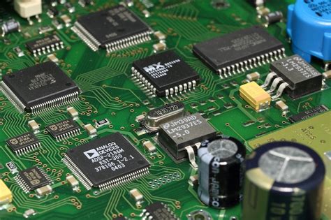
One of the primary functions of a PCB assembly is to provide mechanical support for the various electronic components that make up a circuit. Components like resistors, capacitors, integrated circuits (ICs), and connectors are securely soldered onto the PCB, ensuring they remain in place even when subjected to vibration or physical stress.
The PCB itself is made from a sturdy, non-conductive material, typically fiberglass reinforced epoxy resin (FR4). This material offers excellent mechanical strength and dimensional stability, allowing the PCB to support the components without flexing or warping.
Electrical Connectivity Between Components
The second key function of a PCB assembly is to provide electrical connectivity between the various components on the board. The PCB features conductive traces, usually made of copper, that are etched or printed onto the board’s surface. These traces act as pathways for electrical signals to travel between components, allowing them to interact and perform their intended functions.
In addition to the surface traces, PCBs can have multiple layers, with conductive traces sandwiched between insulating layers. This allows for more complex routing of signals and enables higher component density on the board.
Compact and Efficient Packaging
PCB assemblies offer a compact and efficient way to package electronic circuits. By mounting components directly onto the PCB and using multi-layer designs, designers can create highly dense assemblies that take up minimal space. This is particularly important in applications where size and weight are critical factors, such as in mobile devices, wearables, and aerospace equipment.
The compact nature of PCB assemblies also helps to reduce the overall cost of electronic devices. By minimizing the space required for the circuit, manufacturers can create smaller, more affordable products.
Reliable Operation in Various Environments
A well-designed PCB assembly can provide reliable operation in a wide range of environments. The PCB material and the solder used to attach components are selected to withstand the expected operating conditions, such as temperature fluctuations, humidity, and vibration.
Additionally, PCBs can be coated with protective materials, like conformal coatings, to further enhance their durability and resistance to environmental factors. These coatings help to prevent corrosion, insulate the board from moisture, and protect against physical damage.
Enabling Complex Circuit Designs
PCB assemblies enable the creation of complex circuit designs that would be difficult or impossible to achieve with other methods. The ability to route signals through multiple layers and the precision of the etching process allow for intricate, high-density designs.
Furthermore, PCB design software and manufacturing techniques have advanced to the point where designers can create boards with very fine pitch components, high-speed signals, and controlled impedance. These capabilities are essential for modern applications like high-speed communication systems, advanced sensors, and high-performance computing.
PCB Assembly Methods
There are two primary methods used to assemble PCBs: through-hole and surface mount.
Through-Hole Assembly
Through-hole assembly involves inserting component leads through drilled holes in the PCB and soldering them to pads on the opposite side. This method is often used for larger components or those that require greater mechanical stability.
Advantages of through-hole assembly include:
- Stronger mechanical bonds between components and the PCB
- Easier to inspect and repair manually
- Better suited for high-power applications
Disadvantages include:
- Larger component size and board space requirements
- Higher cost due to manual assembly
- Limited component density compared to surface mount
Surface Mount Assembly
Surface mount assembly involves placing components directly onto pads on the surface of the PCB and soldering them in place. This method allows for much smaller components and higher density designs.
Advantages of surface mount assembly include:
- Smaller component size and higher density designs
- Lower cost due to automated assembly processes
- Improved high-frequency performance
Disadvantages include:
- More difficult to inspect and repair manually
- Requires specialized equipment for assembly
- More susceptible to thermal stress and vibration
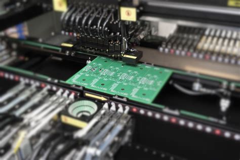
PCB Assembly Process
The PCB assembly process typically involves the following steps:
-
Solder Paste Application: Solder paste, a mixture of tiny solder balls and flux, is applied to the PCB pads using a stencil or screen printing process.
-
Component Placement: Components are placed onto the PCB using automated pick-and-place machines or manually for through-hole components.
-
Reflow Soldering: The PCB is heated in a reflow oven, melting the solder paste and creating a permanent bond between the components and the board.
-
Inspection and Testing: The assembled PCB is inspected visually and tested electrically to ensure proper functionality and quality.
-
Cleaning and Coating: If required, the PCB is cleaned to remove any residual flux and coated with a protective material to enhance durability.

Benefits of PCB Assembly
PCB assembly offers numerous benefits for electronic device manufacturing:
-
Reliability: PCBs provide a stable and reliable platform for electronic circuits, ensuring consistent performance and long-term durability.
-
Cost-effectiveness: The automated nature of PCB assembly processes and the ability to create high-density designs help to reduce manufacturing costs.
-
Scalability: PCB assembly techniques can be easily scaled up for high-volume production, making it an ideal choice for mass-produced electronic devices.
-
Customization: PCBs can be designed and manufactured to meet specific application requirements, allowing for a high degree of customization.
-
Improved performance: The compact nature of PCB assemblies and the ability to create complex, multi-layer designs enable improved electrical performance and signal integrity.
Applications of PCB Assembly
PCB assemblies are used in a wide range of industries and applications, including:
- Consumer electronics (smartphones, tablets, laptops, etc.)
- Automotive electronics (infotainment systems, engine control units, sensors, etc.)
- Medical devices (diagnostic equipment, monitoring systems, implantable devices, etc.)
- Industrial control systems (PLCs, sensors, automation equipment, etc.)
- Aerospace and defense (avionics, communication systems, radar, etc.)
- IoT devices (smart home devices, wearables, remote sensors, etc.)
The versatility and reliability of PCB assemblies make them an essential component in virtually every electronic device we use today.
FAQ
1. What is the difference between a PCB and a PCBA?
A PCB (printed Circuit Board) is the bare board without any components attached. A PCBA (printed circuit board assembly) is a PCB that has been populated with electronic components and is ready for use in an electronic device.
2. What are the most common materials used for PCBs?
The most common material used for PCBs is FR4, a fiberglass reinforced epoxy resin. Other materials include aluminum-backed PCBs for heat dissipation, flexible PCBs made from polyimide or polyester, and high-frequency PCBs made from materials like PTFE or Rogers laminates.
3. What is the difference between through-hole and surface mount assembly?
Through-hole assembly involves inserting component leads through drilled holes in the PCB and soldering them to pads on the opposite side. Surface mount assembly involves placing components directly onto pads on the surface of the PCB and soldering them in place. Surface mount assembly allows for smaller components and higher density designs compared to through-hole.
4. How are PCBAs tested for functionality and quality?
PCBAs are typically tested using a combination of visual inspection, automated optical inspection (AOI), and electrical testing. Visual and AOI inspect the board for defects like solder bridges, component misalignment, or missing components. Electrical testing verifies the functionality of the board and ensures it meets the specified performance requirements.
5. What is the role of a solder mask on a PCB?
A solder mask is a protective layer applied to the surface of a PCB, covering the areas that should not be soldered. It serves several purposes:
- Prevents solder bridges from forming between closely spaced pads
- Protects the copper traces from oxidation and environmental damage
- Provides electrical insulation between conductive areas
- Improves the aesthetics of the PCB by providing a uniform color (often green)
The solder mask is selectively applied, leaving the pads and other areas that require soldering exposed.
Conclusion
PCB assembly is a crucial process in the manufacturing of electronic devices, providing mechanical support, electrical connectivity, and reliable performance in a compact package. The functions of a PCB assembly enable the creation of complex, high-density circuit designs that power the devices we use every day.
As electronic devices continue to advance and evolve, the importance of PCB assembly will only continue to grow. By understanding the functions, methods, and benefits of this essential process, engineers and manufacturers can design and produce more efficient, reliable, and cost-effective electronic products.


Leave a Reply