PCB Assembly Blog
-
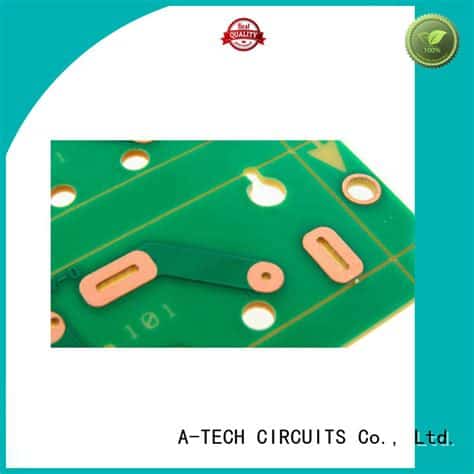
Applying Carbon Contacts to PCBs
Posted by
–
Read more: Applying Carbon Contacts to PCBsIntroduction to PCB-CarbonContacts Printed circuit boards (PCBs) are essential components in modern electronics, providing a platform for interconnecting electronic components. One critical aspect of PCB design and manufacturing is the application of contacts, which enable electrical connections between the PCB and other components or devices. Among the various materials used for PCB contacts, carbon has…
-
Tips & Tricks – Why Do Components Tombstone
Posted by
–
 Read more: Tips & Tricks – Why Do Components Tombstone
Understanding Component Tombstoning Components tombstoning is a phenomenon that occurs in electronic circuits where components stand up or tilt at an angle after being subjected to harsh conditions such as high temperatures during Reflow Soldering. This issue can lead to various problems, including poor electrical connections, reduced mechanical strength, and even complete circuit failure. In…
-
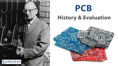
The History of Printed Circuit Boards
Posted by
–
 Read more: The History of Printed Circuit Boards
Introduction to PCB History Printed Circuit Boards (PCBs) have revolutionized the electronics industry since their inception in the early 20th century. These boards, which are used to mechanically support and electrically connect electronic components using conductive pathways, have become an integral part of modern electronics. In this article, we will delve into the fascinating history…
-
 Read more: New options for Chemical Nickel-Gold surface finish
Introduction to Nickel-Gold surface finish Nickel-Gold (Ni-Au) surface finish is a popular choice in the electronics industry for its excellent properties, including high corrosion resistance, good solderability, and compatibility with wire bonding processes. This finish is widely used in applications such as printed circuit boards (PCBs), connectors, and semiconductor packaging. The Nickel-Gold surface finish typically…
-
Multilayer Standard Builds
Posted by
–
 Read more: Multilayer Standard Builds
Introduction to BuildStandards in Manufacturing In modern manufacturing, efficiency and consistency are crucial for success. One key aspect of achieving these goals is the implementation of standardized build processes, also known as BuildStandards. These standards ensure that every product is manufactured using the same methods, materials, and quality control measures, resulting in a more streamlined…
-
PCB & Assembly Services – eC-stencil
Posted by
–
 Read more: PCB & Assembly Services – eC-stencil
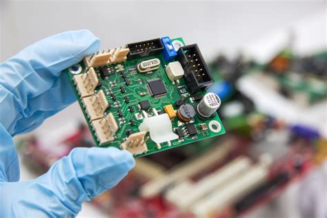
What is PCB Assembly? PCB assembly is the process of soldering or mounting electronic components onto a printed circuit board (PCB). The main purpose of PCB assembly is to create a functional electronic device by interconnecting various components according to a predefined design. PCB assembly involves several steps, including: Solder Paste Application Component Placement Reflow…
-
 Read more: White paper – suitability of an enhanced low melting point alloy for a handheld device.
Introduction The selection of materials is a critical consideration in the design and manufacturing of handheld devices. The choice of alloy can significantly impact the device’s performance, durability, and user experience. In recent years, there has been growing interest in the use of low melting point alloys for various applications, including handheld devices. This white…
-
What is Inner Layer Pad Insulation?
Posted by
–
 Read more: What is Inner Layer Pad Insulation?
What is Pad Insulation? Pad insulation refers to the material used to insulate and protect the inner layers of a printed circuit board (PCB) or other electronic components. It is typically made from dielectric materials that have high electrical resistance and excellent thermal stability. The primary purpose of pad insulation is to prevent short circuits…
-
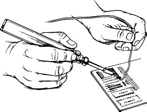 Read more: Hand-soldering – point by point or mini-wave technique
What is point by point soldering? Point by point soldering, also known as touch soldering, is a technique where the soldering iron tip is used to heat both the component lead and the pad on the printed circuit board (PCB) simultaneously. The solder is then applied to the joint, creating a connection between the component…
-
DRC Settings and Guidelines for CAD Packages
Posted by
–
 Read more: DRC Settings and Guidelines for CAD Packages
Introduction to DRC in CAD Design Rule Checking (DRC) is a critical step in the electronic design process that verifies a design meets all manufacturing specifications and will result in a functioning, manufacturable product. DRC identifies design errors, violations of manufacturing constraints, and potential reliability issues. Running DRC checks within a CAD tool before releasing…


