What is a Printed Circuit board (PCB)?
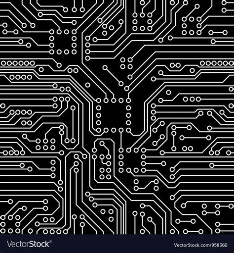
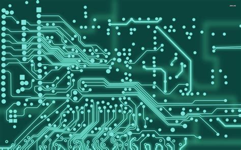
A printed circuit board, or PCB, is a thin board made of fiberglass, composite epoxy, or other laminate material. Conductive pathways are etched or “printed” onto the board, connecting different components on the PCB, such as transistors, resistors, and integrated circuits.
PCBs are designed to support and electrically connect electronic components using conductive tracks, pads, and other features etched from one or more sheet layers of copper laminated onto and/or between sheet layers of a non-conductive substrate.
Components of a PCB
A typical PCB consists of the following components:
-
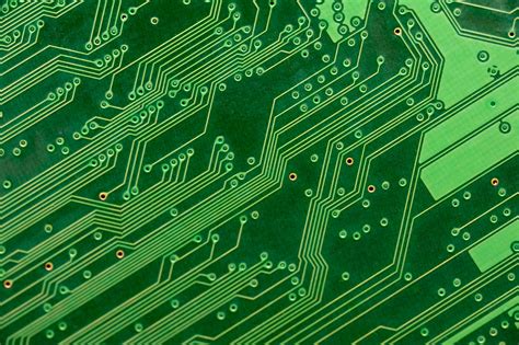
Substrate: The base material of the PCB, which is usually made of fiberglass, composite epoxy, or other laminate material.
-
Copper layers: Thin layers of copper foil that are laminated onto the substrate. The copper is etched to form the conductive tracks, pads, and other features of the circuit board.
-
Solder mask: A thin layer of polymer that is applied over the copper layer to protect it from oxidation and prevent solder bridges from forming between closely spaced solder pads.
-
Silkscreen: A printed layer of text and symbols that identify the components on the PCB and provide other information such as the board’s part number and revision level.
| Component | Description |
|---|---|
| Substrate | The base material of the PCB, usually made of fiberglass, composite epoxy, or other laminate. |
| Copper layers | Thin layers of copper foil laminated onto the substrate, etched to form conductive features. |
| Solder mask | A thin polymer layer applied over the copper to protect it from oxidation and solder bridging. |
| Silkscreen | A printed layer of text and symbols identifying components and providing other information. |
Types of PCBs
There are several types of PCBs, each with its own unique characteristics and applications. The most common types are:
Single-sided PCB
A single-sided PCB has conductive traces on only one side of the substrate. These boards are the simplest and least expensive to manufacture, but they have limitations in terms of circuit density and complexity.
Double-sided PCB
Double-sided PCBs have conductive traces on both sides of the substrate. The two sides are connected using vias, which are small holes drilled through the board and plated with metal. Double-sided PCBs offer higher circuit density and more flexibility in component placement compared to single-sided boards.
Multi-layer PCB
Multi-layer PCBs have three or more conductive layers, alternating with insulating layers. The layers are connected using vias, just like in double-sided PCBs. Multi-layer boards offer the highest circuit density and complexity, making them suitable for advanced applications such as high-speed digital circuits and RF systems.
Flexible PCB
Flexible PCBs, or flex circuits, are made using a flexible substrate material such as polyimide. They can be bent and folded to fit into tight spaces or conform to irregular shapes. Flex circuits are commonly used in applications where space is limited, such as mobile devices, wearables, and medical implants.
Rigid-Flex PCB
Rigid-flex PCBs combine the benefits of rigid and flexible PCBs. They consist of rigid sections connected by flexible sections, allowing for complex 3D shapes and improved reliability in applications with high vibration or mechanical stress.
| PCB Type | Layers | Complexity | Cost | Common Applications |
|---|---|---|---|---|
| Single-sided | 1 | Low | Low | Simple circuits, low-cost consumer products |
| Double-sided | 2 | Medium | Medium | More complex circuits, general electronics |
| Multi-layer | 3+ | High | High | Advanced circuits, high-speed digital, RF systems |
| Flexible | 1-2 | Medium | Medium | Wearables, mobile devices, medical implants |
| Rigid-Flex | 2+ | High | High | Complex 3D shapes, high-reliability applications |
PCB design and Manufacturing Process
The PCB design and manufacturing process involves several steps, from conceptualization to the final product. The main stages are:
-
Schematic design: The circuit is designed using a schematic capture tool, which defines the electrical connections between components.
-
PCB layout: The physical layout of the PCB is created using a PCB layout tool. This involves placing components, routing traces, and defining the board’s dimensions and layer stackup.
-
Design rule check (DRC): The PCB layout is checked against a set of design rules to ensure that it meets manufacturability and reliability requirements.
-
Gerber file generation: The PCB layout is exported as a set of Gerber files, which are the industry standard format for PCB manufacturing.
-
PCB fabrication: The Gerber files are sent to a PCB manufacturer, who fabricates the board using a series of processes including etching, plating, and lamination.
-
PCB assembly: The fabricated PCB is populated with components using automated assembly equipment or manual soldering.
-
Testing and inspection: The assembled PCB is tested and inspected to ensure that it functions as intended and meets quality standards.

Advantages of Using PCBs
PCBs offer several advantages over other wiring methods, such as point-to-point wiring and wire-wrap. Some of the key benefits include:
-
Compact size: PCBs allow for high component density, enabling the creation of compact and lightweight electronic devices.
-
Reliability: The use of PCBs reduces the risk of wiring errors and improves the overall reliability of the circuit.
-
Reproducibility: PCBs are designed using software tools, making it easy to reproduce identical boards for mass production.
-
Cost-effective: The automated manufacturing process for PCBs makes them cost-effective, especially for large-scale production.
-
Improved signal integrity: The precise layout and controlled impedance of PCB traces help maintain signal integrity, which is essential for high-speed and RF applications.
Applications of PCBs
PCBs are used in a wide range of applications across various industries. Some common applications include:
-
Consumer electronics: PCBs are found in smartphones, laptops, televisions, and other household electronic devices.
-
Automotive: Modern vehicles rely heavily on PCBs for various systems, such as engine control, infotainment, and advanced driver assistance systems (ADAS).
-
Medical devices: PCBs are used in medical equipment, such as patient monitors, imaging systems, and implantable devices.
-
Industrial automation: PCBs play a crucial role in industrial control systems, robotics, and process automation equipment.
-
Aerospace and defense: High-reliability PCBs are used in aircraft, satellites, and military equipment, where failure is not an option.
Frequently Asked Questions (FAQ)
-
What is the difference between a PCB and a breadboard?
A breadboard is a reusable prototyping tool that allows you to create temporary circuits without soldering. PCBs, on the other hand, are permanent boards that are designed and manufactured for specific circuits. -
Can I design my own PCB?
Yes, you can design your own PCB using various software tools available in the market, such as Eagle, KiCad, and Altium Designer. However, it is essential to have a good understanding of circuit design and PCB layout principles. -
How much does it cost to manufacture a PCB?
The cost of manufacturing a PCB depends on several factors, such as the board size, layer count, material, and quantity. Small, simple boards can cost a few dollars each, while large, complex boards can cost hundreds of dollars per piece. -
What is the typical turnaround time for PCB manufacturing?
The turnaround time for PCB manufacturing varies depending on the complexity of the board and the manufacturer’s workload. Typical lead times range from a few days to several weeks. -
Are there any environmental concerns associated with PCB manufacturing?
Yes, PCB manufacturing involves the use of hazardous chemicals and materials, such as lead, which can have negative environmental impacts if not properly managed. Many manufacturers now offer lead-free and RoHS-compliant PCBs to address these concerns.
In conclusion, PCBs are the backbone of modern electronics, enabling the creation of compact, reliable, and cost-effective devices. Understanding the basics of PCBs, including their components, types, design process, and applications, is essential for anyone involved in electronics design and manufacturing.


Leave a Reply