The Importance of PCB Design
PCB design is a crucial step in the development of electronic devices. It determines the functionality, reliability, and performance of the final product. A well-designed PCB ensures that the electronic components are connected correctly, minimizes signal interference, and maximizes the device’s efficiency. On the other hand, a poorly designed PCB can lead to device malfunction, short circuits, and even physical damage.
Key Aspects of PCB Design
-
Schematic Design: The first step in PCB design is creating a schematic diagram that represents the electrical connections between components. This involves selecting the appropriate components, determining their values, and defining how they are connected.
-
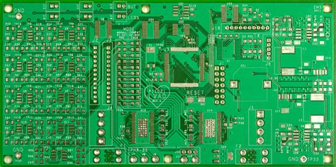
Component Placement: Once the schematic is complete, the next step is to place the components on the PCB layout. This involves considering factors such as component size, shape, and pin configuration, as well as the overall board size and shape.
-
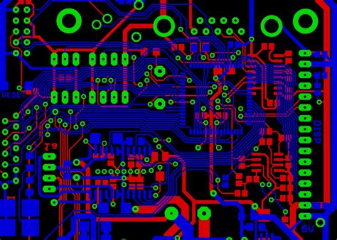
Routing: After component placement, the connections between components are routed using copper traces. This involves determining the optimal path for each connection while avoiding interference and ensuring proper signal integrity.
-
Manufacturing Considerations: PCB design must also take into account the limitations and requirements of the manufacturing process. This includes considerations such as minimum trace width and spacing, hole sizes, and solder mask and silkscreen layers.
PCB Design Tools
There are several software tools available for PCB design, ranging from free open-source options to high-end commercial packages. Some popular PCB design tools include:
| Tool | Description | Pricing |
|---|---|---|
| KiCad | Open-source PCB design suite with schematic capture and PCB layout tools | Free |
| EAGLE | Popular PCB design tool with schematic capture, PCB layout, and CAM tools | Free and paid versions |
| Altium Designer | High-end PCB design package with advanced features for complex designs | Paid |
| OrCAD | Comprehensive PCB design solution with schematic capture, PCB layout, and simulation tools | Paid |
| Autodesk EAGLE | Cloud-based PCB design tool with schematic capture and PCB layout tools | Free and paid versions |
PCB Manufacturing
Once the PCB design is complete, the next step is to manufacture the physical board. This involves several processes, including:
-
PCB Fabrication: The PCB design files are sent to a PCB fabrication house, which creates the physical board using a series of chemical and mechanical processes. This typically involves etching the copper traces, drilling holes, and applying solder mask and silkscreen layers.
-
PCB Assembly: After fabrication, the electronic components are soldered onto the board using either through-hole or surface-mount technology (SMT). This can be done manually for small-scale production or using automated pick-and-place machines for larger volumes.
-
Testing and Inspection: Once the PCB is assembled, it undergoes various tests and inspections to ensure proper functionality and reliability. This may include visual inspections, electrical tests, and environmental stress tests.

PCB Design Considerations
When designing a PCB, there are several key considerations to keep in mind:
Signal Integrity
Signal integrity refers to the quality of the electrical signals transmitted through the PCB. Poor signal integrity can lead to issues such as crosstalk, reflections, and electromagnetic interference (EMI). To ensure good signal integrity, PCB designers must consider factors such as trace width and spacing, impedance matching, and grounding and shielding techniques.
Power Distribution
Proper power distribution is essential for ensuring that all components on the PCB receive the correct voltage and current levels. This involves designing a power distribution network (PDN) that minimizes voltage drops and ensures stable power delivery. Techniques such as power and ground planes, decoupling capacitors, and voltage regulators are commonly used to achieve good power distribution.
Thermal Management
Electronic components generate heat during operation, and excessive heat can lead to performance degradation and even device failure. PCB designers must consider thermal management techniques to ensure that heat is effectively dissipated from the board. This may involve using thermal vias, heat sinks, or active cooling solutions such as fans or thermoelectric coolers.
Manufacturability
PCB design must also consider the limitations and requirements of the manufacturing process. This includes factors such as minimum trace width and spacing, hole sizes, and solder mask and silkscreen layers. Designers must also consider the availability and cost of components, as well as the overall board size and shape.
PCB Design Best Practices
To ensure a successful PCB design, there are several best practices that designers should follow:
-
Start with a clear specification: Before beginning the design process, it is essential to have a clear understanding of the device’s requirements, including its functionality, performance, and environmental conditions.
-
Use a modular design approach: Dividing the PCB into functional modules can simplify the design process and make it easier to make changes or upgrades later on.
-
Follow design rules and guidelines: Adhering to established design rules and guidelines, such as those provided by the IPC (Association Connecting Electronics Industries), can help ensure that the PCB is manufacturable and reliable.
-
Use simulation and analysis tools: Simulation and analysis tools can help identify potential issues early in the design process, such as signal integrity problems or thermal hotspots.
-
Collaborate with manufacturers: Working closely with PCB fabrication and assembly partners can help ensure that the design is optimized for manufacturability and can be produced efficiently and cost-effectively.
Frequently Asked Questions (FAQ)
1. What is the difference between a schematic and a PCB layout?
A schematic is a graphical representation of the electrical connections between components, while a PCB layout is the physical arrangement of those components on the board. The schematic defines the logical connections, while the PCB layout determines the physical placement and routing of those connections.
2. What is the difference between through-hole and surface-mount technology (SMT)?
Through-hole technology involves components with leads that are inserted into holes drilled in the PCB and soldered on the opposite side. SMT involves components that are mounted directly onto the surface of the PCB. SMT allows for smaller components and higher component density, while through-hole technology is more robust and easier to assemble manually.
3. What is a via in PCB design?
A via is a small hole drilled in the PCB that allows a connection to be made between different layers of the board. Vias are used to route signals between layers and to provide thermal and electrical connections between components on different layers.
4. What is the purpose of a solder mask and silkscreen layer?
A solder mask is a layer of polymer that is applied to the PCB to protect the copper traces from oxidation and to prevent solder bridges from forming during assembly. A silkscreen layer is a layer of ink that is applied to the PCB to provide labels and markings for components and other features.
5. What is the typical turnaround time for PCB fabrication and assembly?
The turnaround time for PCB fabrication and assembly can vary depending on the complexity of the design, the manufacturing process, and the vendor. Typical turnaround times range from a few days to several weeks. Rush services are often available for an additional cost.
In conclusion, PCB design is a crucial step in the development of electronic devices. It involves creating a blueprint for the physical layout and electrical connections of a printed circuit board, taking into account factors such as signal integrity, power distribution, thermal management, and manufacturability. By following best practices and collaborating closely with manufacturing partners, PCB designers can ensure that their designs are functional, reliable, and cost-effective.


Leave a Reply