Introduction to Surface Mount Technology
Surface Mount Technology (SMT) has revolutionized the electronics manufacturing industry since its introduction in the 1980s. SMT involves mounting electronic components directly onto the surface of a Printed Circuit Board (PCB), as opposed to the traditional through-hole method where component leads are inserted into holes drilled in the PCB. The electronic components used in SMT are called Surface Mount Devices (SMDs).
SMDs have gained immense popularity due to their compact size, lower cost, and improved performance compared to through-hole components. They have enabled the miniaturization of electronic devices, making them more portable and efficient. Today, SMDs are used in a wide range of applications, from consumer electronics to aerospace and military systems.
Characteristics of Surface Mount Devices
Compact Size
One of the most significant advantages of SMDs is their small size. SMDs are typically 70% smaller than their through-hole counterparts, allowing for higher component density on PCBs. This miniaturization has enabled the development of compact electronic devices such as smartphones, smartwatches, and medical implants.
The table below compares the sizes of some common through-hole components with their SMD equivalents:
| Component | Through-Hole Size | SMD Size |
|---|---|---|
| Resistor | 0.25 W, 6.8 mm | 0603, 1.6 mm x 0.8 mm |
| Capacitor | 2.5 mm lead spacing | 0805, 2.0 mm x 1.25 mm |
| Transistor | TO-92, 4.8 mm lead spacing | SOT-23, 2.9 mm x 1.3 mm |
Lighter Weight
SMDs are significantly lighter than through-hole components due to their smaller size and lack of long leads. This weight reduction is crucial for applications where every gram counts, such as in aerospace and portable devices. Lighter electronic assemblies also contribute to lower shipping costs and reduced environmental impact.
Lower Cost
The cost of SMDs is generally lower than that of through-hole components. This can be attributed to several factors:
- Smaller size: SMDs require less raw material, resulting in lower manufacturing costs.
- Automated assembly: SMT allows for highly automated assembly processes, reducing labor costs and increasing production speeds.
- Fewer drilling operations: SMT eliminates the need for drilling holes in PCBs, saving time and reducing manufacturing costs.
Improved Performance
SMDs offer several performance advantages over through-hole components:
- Reduced parasitic effects: The shorter leads of SMDs minimize parasitic inductance and capacitance, improving high-frequency performance.
- Better thermal management: SMDs have a larger contact area with the PCB, allowing for better heat dissipation and improved thermal management.
- Lower profile: The low profile of SMDs enables the design of slimmer electronic devices and allows for better airflow in densely packed assemblies.

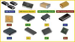
Surface Mount Device Packages
SMDs come in various package styles, each designed for specific applications and manufacturing requirements. Some common SMD packages include:
Chip Components
Chip components, such as resistors and capacitors, are the most basic SMD packages. They are rectangular in shape and have two terminations on opposite sides. Chip components are designated by their size, with common sizes being 0402 (1.0 mm x 0.5 mm), 0603 (1.6 mm x 0.8 mm), and 0805 (2.0 mm x 1.25 mm).
Small Outline Packages (SOPs)
Small Outline Packages (SOPs) are used for integrated circuits (ICs) and have leads on two sides of the package. The number of leads can vary from 8 to 56 or more. Some common SOP variants include:
- Small Outline Integrated Circuit (SOIC): A popular package for general-purpose ICs, with a lead pitch of 1.27 mm.
- Thin Small Outline Package (TSOP): A thinner version of the SOIC, often used for memory devices.
- Shrink Small Outline Package (SSOP): A smaller version of the SOIC, with a lead pitch of 0.635 mm or less.
Quad Flat Packages (QFPs)
Quad Flat Packages (QFPs) have leads on all four sides of the package, allowing for a higher pin count than SOPs. QFPs are commonly used for microcontrollers, digital signal processors (DSPs), and other complex ICs. Some QFP variants include:
- Low-profile Quad Flat Package (LQFP): A thinner version of the QFP, with a lead pitch of 0.5 mm or less.
- Thin Quad Flat Package (TQFP): Similar to the LQFP, but with a slightly thicker profile.
- Quad Flat No-lead (QFN): A leadless package with contacts on the bottom surface, offering a smaller footprint and better thermal performance.
Ball Grid Array (BGA)
Ball Grid Array (BGA) packages have an array of solder balls on the bottom surface, allowing for a high pin count in a compact size. BGAs are used for complex ICs such as microprocessors, FPGAs, and ASICs. The solder balls are typically arranged in a grid pattern with a pitch of 0.5 mm to 1.27 mm.

Surface Mount Device Assembly Process
The SMT assembly process involves several steps, each requiring specialized equipment and materials. The main steps in the SMT assembly process are:
-
Solder Paste Printing: Solder paste, a mixture of tiny solder particles and flux, is applied to the PCB using a stencil or screen printing process. The stencil has openings that match the pads on the PCB, ensuring precise solder paste deposition.
-
Component Placement: SMDs are placed onto the solder paste-covered pads using pick-and-place machines. These machines use vacuum nozzles or grippers to pick up components from reels or trays and place them accurately on the PCB.
-
Reflow Soldering: The PCB with the placed components is then passed through a reflow oven. The oven heats the assembly in a controlled manner, causing the solder paste to melt and form a reliable electrical and mechanical connection between the components and the PCB pads. The reflow temperature profile is carefully designed to ensure proper solder joint formation without damaging the components.
-
Inspection and Testing: After the reflow process, the assembled PCBs are inspected for defects such as bridging, tombstoning, or missing components. Automated optical inspection (AOI) systems are commonly used for this purpose. Functional testing is also performed to ensure that the assembled PCBs meet the required specifications.

Advantages of Surface Mount Technology
SMT offers several advantages over through-hole technology, making it the preferred choice for modern electronic manufacturing:
-
Increased Design Flexibility: SMT allows for higher component density and more complex designs, enabling the development of advanced electronic devices with enhanced functionality.
-
Improved Reliability: SMDs have shorter leads and a larger contact area with the PCB, resulting in better mechanical and thermal stress distribution. This improves the overall reliability of the electronic assembly.
-
Faster Assembly: SMT enables highly automated assembly processes, significantly reducing the time required to assemble a PCB compared to through-hole technology. This leads to faster production times and lower labor costs.
-
Better High-Frequency Performance: SMDs have lower parasitic inductance and capacitance, making them suitable for high-frequency applications such as radio frequency (RF) and microwave circuits.
-
Reduced Environmental Impact: SMT uses less energy and produces less waste compared to through-hole technology. The elimination of drilling operations and the use of lead-free solder also contribute to a more environmentally friendly manufacturing process.
Challenges in Surface Mount Technology
While SMT has numerous advantages, it also presents some challenges that must be addressed for successful implementation:
-
Component Handling: SMDs are small and delicate, requiring specialized handling equipment and techniques to prevent damage during assembly. Proper storage and moisture control are also essential to maintain component integrity.
-
Thermal Management: The high component density in SMT assemblies can lead to increased heat generation. Proper thermal management techniques, such as the use of Thermal Vias and heat sinks, must be employed to ensure reliable operation.
-
Solder Joint Reliability: SMT solder joints are smaller and more numerous than through-hole joints, making them more susceptible to defects such as bridging, voiding, or cracking. Careful process control and the use of advanced solder materials can help mitigate these issues.
-
Rework and Repair: Reworking or repairing SMT assemblies can be challenging due to the small size and close proximity of components. Specialized tools and techniques, such as hot air rework stations and microscopes, are required for effective rework.
-
Electrostatic Discharge (ESD) Protection: Many SMDs, particularly ICs, are sensitive to ESD. Proper ESD protection measures, such as grounding, shielding, and the use of ESD-safe materials, must be implemented throughout the manufacturing process.
Future Trends in Surface Mount Technology
As electronic devices continue to evolve, SMT is also advancing to meet the changing requirements. Some of the future trends in SMT include:
-
Miniaturization: The demand for smaller and more powerful electronic devices is driving the development of even smaller SMD packages, such as 0201 (0.5 mm x 0.25 mm) and 01005 (0.4 mm x 0.2 mm) chip components.
-
Advanced Packaging Technologies: Newer packaging technologies, such as Package-on-Package (PoP) and System-in-Package (SiP), are being developed to further increase component density and functionality.
-
Flexible and Stretchable Electronics: SMT is being adapted for use in flexible and stretchable electronic devices, such as wearables and medical implants. This involves the use of flexible PCBs and specialized SMD packages.
-
3D Printing: The integration of 3D printing technology with SMT is being explored for the rapid prototyping and low-volume production of electronic assemblies.
-
Automation and Industry 4.0: SMT assembly processes are becoming increasingly automated, with the integration of robotics, machine vision, and artificial intelligence. This aligns with the Industry 4.0 paradigm, enabling smart factories and more efficient production.
Frequently Asked Questions (FAQ)
1. What is the difference between SMT and through-hole technology?
SMT involves mounting components directly onto the surface of a PCB, while through-hole technology requires components to be inserted into holes drilled in the PCB. SMT components are smaller, lighter, and offer better performance compared to through-hole components.
2. Can SMDs be soldered by hand?
While it is possible to solder SMDs by hand, it requires a steady hand, good eyesight, and specialized tools such as tweezers and a fine-tipped soldering iron. Hand soldering is generally not recommended for production purposes due to the small size of SMDs and the risk of damaging the components or creating poor solder joints.
3. Are SMDs more expensive than through-hole components?
In general, SMDs are less expensive than through-hole components due to their smaller size, lower material costs, and the ability to be assembled using automated processes. However, the initial investment in SMT assembly equipment can be higher compared to through-hole assembly.
4. How do I identify the value of an SMD component?
Most SMDs use a standardized marking system to indicate their value or part number. For example, chip resistors use a three-digit code that represents their resistance value in ohms. SMD capacitors often use a two-digit code for their capacitance value in picofarads. It is essential to refer to the manufacturer’s datasheet or a code chart to correctly identify the value of an SMD component.
5. Can SMDs be reused after being desoldered from a PCB?
While it is possible to desolder and reuse SMDs, it is generally not recommended. The desoldering process can damage the component or alter its properties, leading to reduced reliability. Additionally, the small size of SMDs makes them more susceptible to mechanical damage during handling. In most cases, it is better to use new components when reworking or repairing an SMT assembly.
Conclusion
Surface Mount Devices have revolutionized the electronics manufacturing industry, enabling the development of smaller, lighter, and more powerful electronic devices. SMT offers numerous advantages over through-hole technology, including increased design flexibility, improved reliability, faster assembly, and better high-frequency performance.
As electronic devices continue to evolve, SMT is also advancing to meet the changing requirements. Miniaturization, advanced packaging technologies, flexible and stretchable electronics, 3D printing, and automation are some of the key trends shaping the future of SMT.
While SMT presents some challenges, such as component handling, thermal management, and solder joint reliability, these can be addressed through proper process control, specialized equipment, and advanced materials.
As the electronics industry continues to grow and innovate, Surface Mount Devices will undoubtedly play a crucial role in enabling the development of cutting-edge technologies that improve our lives and shape our future.


Leave a Reply