What is Reflow Soldering?
Reflow soldering is a process used to attach surface mount electronic components to printed circuit boards (PCBs). It involves applying solder paste to the PCB, placing the components onto the solder paste, and then heating the entire assembly in a reflow oven to melt the solder and form permanent electrical and mechanical connections.
Reflow soldering is widely used in the electronics manufacturing industry for high-volume production of PCB assemblies. It provides a reliable and efficient method for attaching many small components to the board simultaneously.
Advantages of Reflow Soldering
Some key advantages of reflow soldering include:
- High throughput and automation for mass production
- Consistent and repeatable solder joint quality
- Ability to solder many components simultaneously
- Compatibility with small, fine-pitch components
- Fewer defects compared to manual soldering methods
The Reflow Soldering Process
The reflow soldering process consists of several key steps:
- Solder paste printing
- Component placement
- Reflow heating
- Cooling
Let’s examine each of these steps in more detail.
1. Solder Paste Printing
The first step is to apply solder paste to the PCB at the locations where components will be attached. Solder paste is a mixture of tiny solder spheres suspended in flux. The flux helps the solder melt and wet to the surface of the PCB pads and component leads.
Solder paste is typically applied using a stencil printing process:
-
A thin metal stencil is aligned over the PCB. The stencil has cutouts that match the component pad locations.
-
Solder paste is dispensed onto the stencil and a squeegee blade is used to spread the paste across the stencil surface, forcing it through the cutouts and onto the PCB pads.
-
The stencil is then lifted away, leaving precise deposits of solder paste on the PCB in preparation for component placement.
Proper control of the solder paste printing process is critical to achieve the right amount of solder on each pad. Insufficient solder can result in open connections, while excessive solder can lead to bridging or short circuits between adjacent pins.
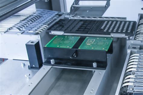
2. Component Placement
After solder paste printing, the next step is to place the surface mount components onto the PCB. This is typically done using automated pick-and-place machines for high speed and precision.
The components are supplied to the machine on tape reels or trays. A robotic head with a vacuum nozzle picks up each component and places it onto the solder paste deposits on the PCB. Optical cameras are used to align the components accurately.
Some key considerations for component placement include:
- Placement accuracy and consistency
- Component orientation and polarity
- Safe handling of static-sensitive and moisture-sensitive devices
- Minimum spacing between components for reflow oven heating
3. Reflow Heating
Once all the components are placed, the populated PCB is run through a reflow oven to melt the solder and permanently attach the parts. The reflow process exposes the entire board to a controlled temperature profile over a period of several minutes.
A typical reflow temperature profile consists of four main phases:
-
Preheat: The board is slowly heated to evaporate solvents in the solder paste and activate the flux. Typical preheat temperatures are 150-180°C.
-
Thermal soak: The board temperature is held steady for 60-120 seconds to allow all areas to reach an even temperature and let the flux remove oxides on the metal surfaces.
-
Reflow: The temperature is rapidly raised above the melting point of the solder alloy, typically to a peak of 240-250°C. The solder spheres melt and wet to the board and component surfaces, forming solder joints. Time above the melting temperature is usually 30-90 seconds.
-
Cooling: The board is cooled back to room temperature, solidifying the molten solder into strong intermetallic bonds. Cooling rates of 2-4°C per second are common.
Here is an example reflow profile graph showing the temperature (y-axis) vs. time (x-axis):
| Time (seconds) | Temperature (°C) | Phase |
|---|---|---|
| 0-90 | 25 to 150 | Preheat |
| 90-210 | 150 to 180 | Thermal soak |
| 210-240 | 180 to 245 | Reflow |
| 240-360 | 245 to 25 | Cooling |
Precise control of the reflow profile is essential to achieve proper solder joint formation without damaging the components or PCB. The ideal profile depends on the solder paste formulation, component specifications, and board characteristics.
4. Cooling
After exiting the reflow oven, the board must be cooled to allow the solder joints to solidify completely. Proper cooling prevents thermal shock to the components and minimizes joint defects like cracks or delamination.
The board is typically cooled by convection in still air or with the assistance of fans. The components, solder joints, and PCB should be cooled at similar rates to avoid mismatches in thermal expansion that could put mechanical stress on the assembly.
While slower cooling is generally better, excessively long cooling times reduce production throughput. Cooling rates of 2-6°C per second are common.

Solder Paste
The solder paste used for reflow soldering is a critical material that has a major impact on process results. Solder paste is a homogeneous mixture of three main ingredients:
-
Solder alloy spheres: Tiny pre-alloyed solder spheres, typically tin-silver-copper (SAC) alloys. Diameters range from 25-45 μm for printing fine features.
-
Flux: A blend of rosins, activators, solvents, and additives that clean metal surfaces, promote solder wetting and flow, and control solder balling and slump.
-
Carrier: A viscous fluid that provides the paste with printable and stable rheological properties. Synthetic resins or castor oil are common carrier bases.
Some key characteristics of solder pastes include:
- Alloy composition and melting temperature
- Sphere size and distribution
- Flux activity and solids content
- Slump and tack properties
- Viscosity and thixotropic index
Solder paste is classified by its alloy type, sphere size, flux type, and viscosity. For example, a common paste might be:
- Sn96.5/Ag3.0/Cu0.5 (SAC305) alloy
- Type 3 (-325/+500 mesh) sphere size
- ROL0 (no-clean) flux
- 900 kcps viscosity
Proper selection and control of solder paste are essential for consistent printability, placement tack, and reflow soldering results.

Reflow Oven Technologies
Reflow ovens used for soldering PCBs come in several different configurations and heating technologies. The three most common types are:
1. Infrared (IR) Ovens
IR reflow ovens use infrared lamps or emitters to heat the board and components. Radiant energy is absorbed and converted to heat within the parts and board, allowing rapid thermal transfer.
Advantages of IR ovens include:
– Fast heating rates
– Good control and profiling capability
– Lower cost than convection ovens
Disadvantages include:
– Uneven heating of components with varying colors and surface finishes
– Shadowing effects on tall components or densely populated areas
– Difficulty heating assemblies inside metal shields or covers
IR ovens are a good fit for simpler, lower-density PCB designs without thermally sensitive parts.
2. Forced Convection Ovens
Convection reflow ovens use hot air flow to transfer heat to the board and components. High-velocity air is circulated through resistive heating elements and then across the moving PCB Assembly.
Advantages of convection ovens include:
– Even distribution of heat across the PCB
– Reduced shadowing and color-dependent effects
– Better suited for dense assemblies and metal housings
– Compatibility with moisture- and thermally sensitive components
Disadvantages include:
– Slower heating rates than IR
– Higher cost and complexity than IR
– More difficult to profile and optimize than IR
Forced convection is the most popular reflow technology for general PCB assembly due to its versatility across a range of board designs.
3. Vapor Phase Ovens
Vapor phase reflow uses a tank of boiling inert fluid (typically perfluoropolyether) to surround the PCB assembly with vapor at a constant temperature. As the vapor condenses on the cooler board, it transfers its latent heat of vaporization to quickly and evenly heat the entire assembly to the boiling point of the fluid.
Advantages of vapor phase include:
– Rapid, uniform heating of complex assemblies
– Inherent temperature control at the fluid boiling point
– No shadowing, color, or surface finish effects
– Minimal ΔT between components and board
Disadvantages include:
– Higher equipment and operating costs
– Fixed peak temperature without cooling zones
– Environmental and safety concerns with fluids
– Slower cycle times and lower throughput
Vapor phase reflow is often used for densely populated, thermally challenging designs that require very even heating and low thermal gradients.

Reflow Soldering Defects
Like any manufacturing process, reflow soldering can produce defects that impact circuit quality and reliability. Some common reflow defects include:
1. Bridging
Solder bridging is a short circuit caused by unintended solder connections between two or more leads. Bridging often results from excessive solder paste deposition, poor stencil design, or component misalignment.
2. Tombstoning
Tombstoning, also known as drawbridging, is a defect where a small two-leaded component stands up on one end, lifting the other end off the PCB. It is caused by uneven surface tension forces during reflow, often due to unequal pad sizes or heating.
3. Open Joints
An open solder joint has incomplete or missing solder connections between the component and PCB pad. Opens can be caused by insufficient solder paste, poor wetting, or solder dewetting and balling.
4. Head-in-Pillow
Head-in-pillow (HIP) defects occur when the solder paste on the PCB pad melts but doesn’t fuse with the solder ball on a BGA component. The result is an open circuit under the component ball that is difficult to detect.
5. Voiding
Solder voids are hollow cavities that form within a solder joint during reflow. Voids weaken the joint mechanically and thermally, and in extreme cases can cause open circuits. Voids often result from flux entrapment or moisture escaping from the PCB or component.
Proper control of the solder paste printing, component placement, and reflow profile is essential to minimize these and other soldering defects.
FAQ
What is the difference between reflow and wave soldering?
Reflow soldering is used to attach surface mount components to the top side of a PCB, while wave soldering is used for through-hole components on the bottom side. In reflow soldering, the entire board is heated to melt pre-deposited solder paste, while in wave soldering the board is passed over a molten solder wave to coat the component leads.
Can reflow soldering be used for through-hole components?
In general, no. Reflow soldering is designed for surface mount components that sit flat on the PCB surface. Through-hole components require a wave soldering or hand soldering process to fill the holes with solder. However, some through-hole parts like connectors can be reflow soldered using special paste-in-hole techniques.
What is the most common solder alloy used for reflow?
The most widely used reflow soldering alloy is Sn96.5/Ag3.0/Cu0.5, also known as SAC305. This lead-free tin-silver-copper alloy melts at 217-220°C and provides a good balance of strength, wetting, and reliability. Other common lead-free alloys include Sn99.3/Cu0.7 (SAC107) and Sn95.5/Ag3.8/Cu0.7 (SAC387).
How do you control the reflow profile in a soldering oven?
Reflow ovens have multiple independently controlled heating zones that can be set to different temperatures and conveyance speeds. This allows the oven to be “profiled” to achieve a desired time-temperature curve. Small PCB assemblies with embedded thermocouples are often run through the oven to measure and optimize the profile for a particular product.
What is the typical defect rate for a reflow soldering process?
The achievable defect rate depends on many factors such as PCB design, Component Types, solder paste material, and process controls. A mature, well-controlled reflow process can typically achieve defect rates below 100 ppm (parts per million), or less than one defect per 10,000 solder joints.
However, more complex assemblies with fine-pitch components may have higher defect rates, while simpler designs can achieve lower rates. Post-reflow inspection and rework are often used to catch and correct defects.


Leave a Reply