How Does ViaFilling Work?
The ViaFilling process typically involves the following steps:
-
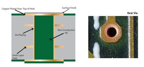
Drilling: Small holes, known as vias, are drilled through the PCB substrate to create electrical connections between different layers.
-
Cleaning: The drilled vias are cleaned to remove any debris or contaminants that may interfere with the filling process.
-
Plating: A thin layer of copper is electroplated onto the walls of the vias to ensure proper electrical conductivity.
-
Filling: The vias are filled with a conductive material, such as copper or a copper alloy, using a specialized filling process.
-
Planarization: The filled vias are planarized (leveled) to ensure a smooth and uniform surface for subsequent manufacturing steps.
The most common methods used for ViaFilling include:
-
Electroplating: This method involves depositing a layer of copper onto the walls of the vias using an electric current. The copper builds up until it completely fills the vias.
-
Screen Printing: A conductive paste is screen printed onto the surface of the PCB, filling the vias. The paste is then cured to create a solid, conductive fill.
-
Conductive Ink Printing: Similar to screen printing, a conductive ink is deposited into the vias using an inkjet printer. The ink is then cured to form a solid fill.
Benefits of ViaFilling
ViaFilling offers several key benefits in PCB manufacturing:
-
Improved Reliability: Filled vias provide a more robust and reliable electrical connection between layers, reducing the risk of failures due to thermal stress or mechanical strain.
-
Enhanced Thermal Management: Filled vias act as thermal conduits, helping to dissipate heat more efficiently from high-power components on the PCB.
-
Increased Design Flexibility: ViaFilling allows for the creation of high-density interconnects, enabling more complex and compact PCB Designs.
-
Better Signal Integrity: Filled vias minimize the impact of signal reflections and crosstalk, improving overall signal integrity in high-speed applications.
-
Reduced Manufacturing Costs: By eliminating the need for additional drilling and plating steps, ViaFilling can help reduce overall manufacturing costs.

Applications of ViaFilling
ViaFilling is used in a wide range of PCB applications, particularly those that require high reliability, thermal management, or high-density interconnects. Some common applications include:
-
Aerospace and Defense: PCBs used in aerospace and defense applications often require high reliability and the ability to withstand extreme environmental conditions. ViaFilling helps ensure the integrity of electrical connections in these demanding applications.
-
Automotive Electronics: As automotive systems become increasingly complex and reliant on electronics, ViaFilling plays a crucial role in ensuring the reliability and performance of PCBs used in vehicles.
-
High-Power Electronics: PCBs used in high-power applications, such as power supplies and motor controls, benefit from the improved thermal management provided by filled vias.
-
High-Speed Digital Devices: Devices that operate at high frequencies, such as smartphones, tablets, and laptops, rely on ViaFilling to maintain signal integrity and minimize signal loss.
-
Medical Devices: PCBs used in medical devices must meet stringent reliability and performance requirements. ViaFilling helps ensure the long-term reliability of these critical components.

Challenges and Considerations
While ViaFilling offers numerous benefits, there are also several challenges and considerations to keep in mind:
-
Material Selection: Choosing the right conductive material for Via Filling is essential to ensure proper electrical conductivity, thermal management, and compatibility with the PCB substrate and other components.
-
Process Control: Achieving consistent and reliable via filling requires careful control of the filling process, including parameters such as temperature, pressure, and fill depth.
-
Design Considerations: PCB designers must consider the specific requirements of ViaFilling when creating layouts, such as via size, spacing, and location.
-
Cost: While ViaFilling can help reduce overall manufacturing costs, the process itself can be more expensive than traditional PCB Fabrication methods.
-
Environmental Impact: Some ViaFilling materials and processes may have environmental implications that must be considered and addressed.

The Future of ViaFilling
As PCB technology continues to advance, the importance of ViaFilling is likely to grow. Some potential future developments in ViaFilling include:
-
Advanced Materials: Researchers are continually developing new conductive materials that offer improved performance, reliability, and environmental compatibility.
-
3D Printing: The integration of 3D printing technologies with ViaFilling could enable the creation of even more complex and high-density PCB structures.
-
Automation: Advances in automation and process control could help improve the consistency, reliability, and cost-effectiveness of ViaFilling processes.
-
Miniaturization: As electronic devices continue to shrink in size, ViaFilling will play an increasingly important role in enabling the creation of ultra-compact, high-density PCBs.
ViaFilling vs. Other Via Formation Methods
ViaFilling is just one of several methods used to create electrical connections between layers in a PCB. Other common methods include:
| Method | Description | Advantages | Disadvantages |
|---|---|---|---|
| Via Plugging | Vias are filled with a non-conductive material, such as epoxy or resin. | – Lower cost than ViaFilling – Provides mechanical support |
– No electrical connection between layers – Limited thermal management benefits |
| Blind/Buried Vias | Vias are drilled and plated, but do not extend through the entire thickness of the PCB. | – Allows for higher density interconnects – Improves signal integrity |
– Higher cost than through-hole vias – More complex manufacturing process |
| Microvias | Very small vias (typically less than 150µm in diameter) are used to create high-density interconnects. | – Enables ultra-high density PCBs – Improved signal integrity |
– Higher cost than larger vias – Requires specialized manufacturing equipment |
Frequently Asked Questions (FAQ)
- What is the difference between ViaFilling and via plugging?
-
ViaFilling involves filling vias with a conductive material to create electrical connections between layers, while via plugging uses a non-conductive material to provide mechanical support without electrical connectivity.
-
Can ViaFilling be used in multi-layer PCBs?
-
Yes, ViaFilling is commonly used in multi-layer PCBs to create reliable electrical connections between different layers.
-
How does ViaFilling improve thermal management in PCBs?
-
Filled vias act as thermal conduits, helping to transfer heat more efficiently from high-power components to other layers or heatsinks, improving overall thermal management.
-
Is ViaFilling more expensive than traditional PCB fabrication methods?
-
While ViaFilling can help reduce overall manufacturing costs by eliminating the need for additional drilling and plating steps, the process itself can be more expensive than traditional methods.
-
What are some common materials used for ViaFilling?
- Common materials used for ViaFilling include copper, copper alloys, and conductive pastes or inks. The choice of material depends on the specific requirements of the application, such as electrical conductivity, thermal management, and compatibility with the PCB substrate.
Conclusion
ViaFilling is a critical technology in modern PCB manufacturing, enabling the creation of high-density interconnects, improved thermal management, and enhanced reliability. As electronic devices continue to become more complex and compact, the importance of ViaFilling will only continue to grow. By understanding the benefits, challenges, and future developments in ViaFilling, PCB designers and manufacturers can stay at the forefront of this essential technology.


Leave a Reply