The Importance of Via Filling in PCB Manufacturing
Via filling plays a crucial role in modern PCB manufacturing for several reasons:
-
Electrical Conductivity: Filling vias with a conductive material ensures that electrical signals can pass through the holes without interruption, maintaining the integrity of the circuit.
-
Mechanical Strength: Filled vias provide additional mechanical support to the PCB, preventing the board from warping or bending during the manufacturing process or in use.
-
Thermal Management: In high-power applications, filled vias can help dissipate heat more efficiently by providing a thermal pathway between layers.
-
Signal Integrity: Filled vias can reduce signal reflections and improve signal integrity, especially in high-frequency applications.
-
Manufacturing Efficiency: Via filling allows for the creation of multi-layer PCBs with a higher density of components, enabling more compact and efficient designs.
Via Filling Techniques
There are several techniques used for via filling in PCB manufacturing, each with its own advantages and limitations. The choice of technique depends on factors such as the size of the vias, the desired level of conductivity, and the manufacturing capabilities of the PCB fabricator.
Electroplating
Electroplating is one of the most common methods for via filling. In this process, the PCB is immersed in an electrolytic solution containing dissolved copper ions. An electric current is applied, causing the copper ions to deposit onto the walls of the vias, gradually filling them. The process continues until the vias are completely filled with copper.
Advantages of electroplating include:
- High conductivity
- Uniform filling
- Suitable for small via diameters
- Cost-effective for high-volume production
Limitations of electroplating include:
- Longer processing times compared to other methods
- Requires precise control of the plating parameters
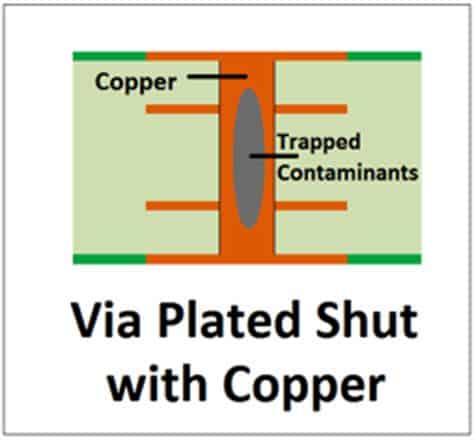
- May result in voids or air pockets if not properly controlled
Conductive Paste Filling
Conductive paste filling involves using a screen printing process to fill the vias with a conductive paste, typically a mixture of copper or silver particles suspended in a polymer binder. After printing, the PCB is heated to cure the paste, creating a solid, conductive fill.
Advantages of conductive paste filling include:
- Faster processing times compared to electroplating
- Suitable for larger via diameters
- Reduced risk of voids or air pockets
Limitations of conductive paste filling include:
- Lower conductivity compared to electroplated copper
- May require multiple printing and curing cycles for complete filling
- Limited to larger via sizes due to the viscosity of the paste
Sintered Via Filling
Sintered via filling is a relatively new technique that combines aspects of both electroplating and conductive paste filling. In this process, a copper paste is screen printed into the vias, and then the PCB is heated to a high temperature in a controlled atmosphere. The heat causes the copper particles to sinter, or fuse together, creating a solid, highly conductive fill.
Advantages of sintered via filling include:
- High conductivity, comparable to electroplated copper
- Fast processing times
- Suitable for a wide range of via sizes
- Reduced risk of voids or air pockets
Limitations of sintered via filling include:
- Higher equipment and processing costs compared to other methods
- Requires precise control of the sintering parameters
- Limited availability among PCB fabricators

Via Filling in Multi-Layer PCBs
Multi-layer PCBs are essential for modern electronics, enabling the creation of complex circuits with high component densities. Via filling plays a critical role in the manufacturing of multi-layer PCBs, as it allows for the creation of reliable electrical connections between layers.
In a typical multi-layer PCB, vias can be classified into three main types:
-
Through Vias: These vias pass through all layers of the PCB, providing electrical connections between the top and bottom layers, as well as any inner layers.
-
Blind Vias: Blind vias are drilled from either the top or bottom layer of the PCB and terminate at an inner layer, providing connections between the surface and one or more inner layers.
-
Buried Vias: Buried vias are located entirely within the inner layers of the PCB and do not extend to the surface layers. They provide connections between adjacent inner layers.
The choice of via type depends on the specific design requirements of the PCB, such as the number of layers, the routing density, and the signal integrity constraints.
When manufacturing multi-layer PCBs with filled vias, the fabrication process typically involves the following steps:
- Drilling the vias using a computer-controlled drill machine
- Desmearing the via walls to remove any debris and improve adhesion
- Applying a seed layer of conductive material, typically copper, to the via walls
- Filling the vias using one of the techniques described earlier (electroplating, conductive paste filling, or sintered via filling)
- Planarizing the surface of the PCB to remove any excess fill material
- Repeating the process for each layer of the PCB, as necessary
By carefully controlling each step of the fabrication process, PCB manufacturers can ensure that the filled vias provide reliable electrical connections between layers, while maintaining the desired mechanical and thermal properties of the board.

Design Considerations for Via Filling
When designing a PCB that requires via filling, several factors must be considered to ensure optimal performance and manufacturability:
-
Via Size: The size of the vias should be chosen based on the specific requirements of the design, such as the current carrying capacity, the routing density, and the manufacturing capabilities of the PCB fabricator. Smaller vias are generally more challenging to fill reliably, while larger vias may consume more board space.
-
Via Placement: The placement of vias should be optimized to minimize the impact on signal integrity and to ensure adequate spacing for the filling process. Vias should be placed away from critical signal traces and should be spaced sufficiently apart to prevent any interactions between adjacent vias during filling.
-
Via Aspect Ratio: The aspect ratio of a via refers to the ratio of its depth to its diameter. High aspect ratio vias (deep and narrow) are more challenging to fill reliably than low aspect ratio vias (shallow and wide). The maximum achievable aspect ratio depends on the specific filling technique and the capabilities of the PCB fabricator.
-
Material Selection: The choice of fill material should be based on the specific requirements of the application, such as the desired level of conductivity, the thermal management needs, and the compatibility with the other materials used in the PCB. Copper is the most common fill material, but other materials such as silver, gold, or conductive polymers may be used in specific applications.
-
Manufacturing Constraints: The design of the PCB should take into account the manufacturing constraints of the chosen fabrication process, such as the minimum via size, the maximum aspect ratio, and the tolerances for via placement and filling. Close collaboration with the PCB fabricator is essential to ensure that the design can be manufactured reliably and cost-effectively.
By carefully considering these factors and working closely with the PCB fabricator, designers can create PCBs with filled vias that meet the specific requirements of their applications while ensuring optimal performance and reliability.

Via Filling Standards and Quality Control
To ensure the quality and reliability of PCBs with filled vias, several industry standards and quality control measures have been established.
IPC Standards
The IPC (Association Connecting Electronics Industries) is a global trade association that develops standards for the electronic interconnection industry. Several IPC standards are relevant to via filling, including:
- IPC-6012: Qualification and Performance Specification for Rigid Printed Boards
- IPC-A-600: Acceptability of Printed Boards
- IPC-4761: Design Guide for Protection of Printed Board Via Structures
These standards provide guidelines for the design, fabrication, and inspection of PCBs with filled vias, helping to ensure consistent quality and reliability across the industry.
Quality Control Measures
PCB fabricators employ various quality control measures to ensure that filled vias meet the required specifications and performance criteria. Some common quality control techniques include:
-
Cross-Sectional Analysis: A sample of the PCB is cut and polished to expose the cross-section of the filled vias. The cross-section is then examined under a microscope to check for voids, cracks, or other defects in the fill material.
-
Electrical Testing: The electrical continuity and resistance of the filled vias are tested using specialized equipment to ensure that they meet the specified performance criteria.
-
Thermal Cycling: The PCB is subjected to multiple cycles of heating and cooling to simulate the thermal stresses that it may experience during operation. This test helps to identify any potential issues with the mechanical integrity of the filled vias.
-
Visual Inspection: The surface of the PCB is visually inspected for any signs of defects or irregularities in the filled vias, such as incomplete filling, protruding fill material, or discoloration.
By adhering to industry standards and implementing rigorous quality control measures, PCB fabricators can ensure that PCBs with filled vias consistently meet the required performance and reliability criteria.
Benefits of Via Filling for Specific Applications
Via filling offers several benefits for specific applications that require high-performance PCBs:
High-Frequency Applications
In high-frequency applications, such as RF and microwave circuits, signal integrity is of utmost importance. Filled vias help to reduce signal reflections and improve signal integrity by providing a low-impedance path for the signals to pass through the PCB. By minimizing signal distortion and losses, filled vias enable the design of high-frequency PCBs with improved performance and reliability.
High-Power Applications
In high-power applications, such as power electronics and motor drives, thermal management is a critical concern. Filled vias provide an efficient thermal pathway for dissipating heat from the components on the surface of the PCB to the inner layers and the heatsink. By improving the thermal conductivity of the PCB, filled vias help to prevent overheating and ensure the long-term reliability of the system.
High-Density Applications
In high-density applications, such as smartphones, wearables, and IoT devices, PCB space is at a premium. Filled vias enable the design of multi-layer PCBs with a higher density of components and interconnects, allowing for more compact and efficient layouts. By maximizing the utilization of the available board space, filled vias help to reduce the overall size and cost of the PCB.
Automotive and Aerospace Applications
In automotive and aerospace applications, PCBs are subjected to harsh environmental conditions, such as extreme temperatures, vibrations, and shocks. Filled vias provide additional mechanical support to the PCB, helping to prevent warping, cracking, or delamination of the layers under these stressful conditions. By improving the structural integrity of the PCB, filled vias contribute to the overall reliability and durability of the electronic system.
By leveraging the benefits of via filling, designers can create PCBs that are optimized for specific applications, delivering improved performance, reliability, and cost-effectiveness.
Frequently Asked Questions (FAQ)
- What is the difference between via filling and via plating?
Via filling and via plating are related but distinct processes in PCB manufacturing. Via plating involves coating the walls of the via with a thin layer of conductive material, typically copper, to create an electrical connection between layers. Via filling, on the other hand, involves completely filling the via with a conductive material to create a solid, continuous electrical and thermal path.
- Can all PCB vias be filled?
Not all PCB vias can be filled, as the ability to fill a via depends on its size, aspect ratio, and the capabilities of the PCB fabricator. In general, smaller vias with higher aspect ratios are more challenging to fill reliably. It is important to consult with the PCB fabricator to determine the feasibility of filling specific via sizes and geometries.
- What materials are commonly used for via filling?
The most common material used for via filling is copper, due to its high electrical and thermal conductivity, as well as its compatibility with standard PCB manufacturing processes. Other materials, such as silver, gold, or conductive polymers, may be used in specific applications that require different properties or performance characteristics.
- How does via filling affect the cost of PCB manufacturing?
Via filling generally increases the cost of PCB manufacturing compared to non-filled vias, due to the additional processing steps and materials required. The cost impact depends on factors such as the number and size of the vias, the chosen filling technique, and the volume of the PCB production run. However, the improved performance and reliability offered by filled vias can often justify the added cost in high-performance applications.
- Are there any limitations or challenges associated with via filling?
Yes, there are several limitations and challenges associated with via filling, including:
- Limited via sizes and aspect ratios that can be reliably filled
- Potential for voids, cracks, or other defects in the fill material
- Increased manufacturing complexity and cost compared to non-filled vias
- Compatibility issues between the fill material and other PCB materials
- Limited availability of certain filling techniques among PCB fabricators
To overcome these challenges, designers must work closely with the PCB fabricator to optimize the via design, choose the appropriate filling technique, and ensure adequate quality control measures are in place.
Conclusion
Via filling is a critical process in the manufacturing of high-performance PCBs, enabling the creation of reliable electrical and thermal connections between layers. By filling the vias with a conductive material, designers can improve signal integrity, thermal management, and mechanical strength, while enabling more compact and efficient PCB layouts.
Several via filling techniques are available, including electroplating, conductive paste filling, and sintered via filling, each with its own advantages and limitations. The choice of technique depends on factors such as the via size, the desired performance characteristics, and the manufacturing capabilities of the PCB fabricator.
To ensure the quality and reliability of PCBs with filled vias, designers must carefully consider several factors, such as via size, placement, aspect ratio, and material selection, and work closely with the PCB fabricator to optimize the design for manufacturability. Adherence to industry standards and rigorous quality control measures are essential for consistently producing high-quality PCBs with filled vias.
As electronic systems continue to push the boundaries of performance, density, and reliability, via filling will remain an essential tool in the PCB designer’s toolkit, enabling the creation of advanced, high-performance PCBs for a wide range of applications.
| Via Filling Technique | Advantages | Limitations |
|---|---|---|
| Electroplating | – High conductivity – Uniform filling – Suitable for small via diameters – Cost-effective for high-volume production |
– Longer processing times – Requires precise control of plating parameters – Potential for voids or air pockets |
| Conductive Paste Filling | – Faster processing times – Suitable for larger via diameters – Reduced risk of voids or air pockets |
– Lower conductivity than electroplated copper – May require multiple printing and curing cycles – Limited to larger via sizes |
| Sintered Via Filling | – High conductivity, comparable to electroplated copper – Fast processing times – Suitable for a wide range of via sizes – Reduced risk of voids or air pockets |
– Higher equipment and processing costs – Requires precise control of sintering parameters – Limited availability among PCB fabricators |


Leave a Reply