Introduction to Thermal Vias
Thermal vias are an essential component in the design and manufacture of printed circuit boards (PCBs). They play a crucial role in managing heat dissipation, ensuring the proper functioning and longevity of electronic components. In this comprehensive article, we will delve into the world of thermal vias, exploring their definition, purpose, types, design considerations, and their significance in various applications.
Definition of Thermal Vias
A thermal via is a small, plated hole that is drilled through a PCB to provide a conductive path for heat to dissipate from a component to the other side of the board or to a heatsink. These vias are typically filled with a conductive material, such as copper, to enhance their thermal conductivity.
Purpose of Thermal Vias
The primary purpose of thermal vias is to transfer heat away from electronic components, such as high-power LEDs, processors, and power transistors. By providing an efficient pathway for heat dissipation, thermal vias help to prevent components from overheating, which can lead to performance degradation, reduced lifespan, or even complete failure.
Types of Thermal Vias
There are several types of thermal vias, each designed to address specific heat dissipation requirements. Let’s explore the most common types:
Filled Thermal Vias
Filled thermal vias are completely filled with a conductive material, typically copper. This filling process enhances the thermal conductivity of the via, allowing for more efficient heat transfer. Filled thermal vias are commonly used in high-power applications or when a component requires a significant amount of heat dissipation.
Plated Thermal Vias
Plated thermal vias have a conductive plating, usually copper, on the inner walls of the hole. The plating thickness can vary depending on the specific requirements of the application. Plated thermal vias provide a balance between thermal conductivity and cost-effectiveness, making them suitable for a wide range of applications.
Capped Thermal Vias
Capped thermal vias are similar to filled thermal vias, but instead of being completely filled, they have a conductive cap on one or both ends of the via. This capping process helps to prevent the formation of voids or air gaps, which can impede heat transfer. Capped thermal vias offer a compromise between the thermal performance of filled vias and the cost-effectiveness of plated vias.

Design Considerations for Thermal Vias
When incorporating thermal vias into a PCB design, several key factors must be considered to ensure optimal performance and manufacturability. Let’s explore these considerations in detail:
Via Size and Spacing
The size and spacing of thermal vias play a crucial role in their effectiveness. Smaller vias allow for more vias to be placed in a given area, increasing the overall thermal conductivity. However, smaller vias also pose manufacturing challenges and may increase production costs. The spacing between vias should be carefully considered to ensure proper heat dissipation while maintaining the structural integrity of the PCB.
Via Placement
The placement of thermal vias is critical to their performance. Vias should be strategically located near the heat-generating components to provide the most direct path for heat dissipation. In some cases, thermal vias may be placed in a grid pattern or a specific arrangement to optimize heat transfer. The placement of vias should also consider the routing of other signal traces to avoid interference or signal integrity issues.
Material Selection
The choice of materials for thermal vias and the surrounding PCB layers can significantly impact their thermal performance. Copper is the most common material used for thermal vias due to its high thermal conductivity. The thickness of the copper plating or filling should be carefully selected based on the heat dissipation requirements and the manufacturing capabilities.
The PCB substrate material also plays a role in heat dissipation. High-performance substrates, such as aluminum or ceramic-based materials, offer better thermal conductivity compared to standard FR-4 substrates. However, these materials may increase the overall cost of the PCB.
Thermal Interface Materials
Thermal interface materials (TIMs) are often used in conjunction with thermal vias to enhance heat transfer between components and the PCB. TIMs, such as thermal pads, thermal pastes, or thermal adhesives, help to fill any air gaps and improve thermal conductivity. The selection of an appropriate TIM depends on factors such as the component’s power dissipation, the available space, and the required thermal performance.

Applications of Thermal Vias
Thermal vias find applications in various industries and electronic devices. Let’s explore some common applications:
Power Electronics
In power electronics, such as switching power supplies, motor drives, and inverters, thermal vias are crucial for managing the heat generated by high-power components like MOSFETs, IGBTs, and rectifiers. Effective heat dissipation through thermal vias ensures the reliable operation of these components and prevents thermal runaway.
LED Lighting
High-power LEDs generate a significant amount of heat, which must be efficiently dissipated to maintain their performance and longevity. Thermal vias are used in LED PCBs to transfer heat from the LED package to the heatsink or other cooling solutions. Proper thermal management through thermal vias ensures stable light output, color consistency, and extended lifespan of LED lighting systems.
Automotive Electronics
Automotive electronics, such as engine control units (ECUs), power steering modules, and infotainment systems, operate in harsh environments with high temperatures and vibrations. Thermal vias are employed in automotive PCBs to dissipate heat from critical components, ensuring their reliable operation and preventing premature failures. The use of thermal vias helps to meet the stringent reliability and safety requirements of the automotive industry.
Consumer Electronics
Consumer electronics, including smartphones, tablets, laptops, and gaming consoles, face the challenge of packing high-performance components into compact form factors. Thermal vias are used in these devices to dissipate heat from processors, graphics chips, and other heat-generating components. Effective thermal management through thermal vias helps to prevent throttling, ensure optimal performance, and enhance the user experience.

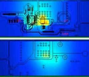
Thermal Via Simulation and Analysis
To optimize the design and placement of thermal vias, engineers rely on simulation and analysis tools. These tools help to predict the thermal performance of the PCB and identify potential hotspots or areas of concern. Let’s explore some common simulation and analysis techniques:
Finite Element Analysis (FEA)
Finite Element Analysis (FEA) is a numerical method used to simulate the thermal behavior of a PCB. FEA tools divide the PCB into small elements and solve complex heat transfer equations to predict temperature distributions and identify thermal bottlenecks. FEA simulations help engineers optimize the placement and size of thermal vias, ensuring effective heat dissipation and preventing thermal issues.
Computational Fluid Dynamics (CFD)
Computational Fluid Dynamics (CFD) is used to simulate the airflow and convective heat transfer around the PCB and its components. CFD tools analyze the interaction between the PCB, thermal vias, and the surrounding environment, considering factors such as air velocity, temperature gradients, and component placement. CFD simulations help to optimize the overall thermal management strategy, including the design of heatsinks and cooling solutions.
Thermal Resistance Network Modeling
Thermal resistance network modeling is a simplified approach to analyze the heat transfer pathways in a PCB. In this method, the PCB is represented as a network of thermal resistances, with thermal vias acting as low-resistance paths for heat flow. This modeling technique allows engineers to quickly estimate the thermal performance of the PCB and make design decisions based on the results.
Best Practices for Thermal Via Design
To ensure the optimal performance and reliability of thermal vias, consider the following best practices:
-
Conduct thorough thermal analysis: Perform thermal simulations and analysis to identify potential hotspots and optimize the placement and design of thermal vias.
-
Use appropriate via size and spacing: Select the appropriate via size and spacing based on the heat dissipation requirements and manufacturing capabilities. Smaller vias and tighter spacing can enhance thermal performance but may increase manufacturing costs.
-
Consider Via Filling or capping: Filled or capped thermal vias offer better thermal conductivity compared to plated vias. Evaluate the trade-offs between thermal performance and manufacturing complexity when deciding on via filling or capping.
-
Optimize via placement: Place thermal vias strategically near heat-generating components to provide the most direct path for heat dissipation. Consider the routing of other signal traces to avoid interference or signal integrity issues.
-
Select suitable materials: Choose PCB substrate materials and copper thicknesses that provide the required thermal conductivity and meet the design constraints. High-performance materials may offer better thermal performance but can increase costs.
-
Use thermal interface materials: Employ thermal interface materials, such as thermal pads or pastes, to enhance heat transfer between components and the PCB. Select the appropriate TIM based on the specific application requirements.
-
Collaborate with manufacturing partners: Work closely with PCB manufacturers to ensure the manufacturability and reliability of thermal via designs. Discuss any specific requirements or constraints early in the design process to avoid potential issues during production.
Frequently Asked Questions (FAQ)
- What is the difference between a thermal via and a regular via?
-
A thermal via is specifically designed to transfer heat from a component to the other side of the PCB or to a heatsink. Regular vias, on the other hand, are primarily used for electrical connections between layers of the PCB.
-
How do I determine the appropriate size and spacing for thermal vias?
-
The size and spacing of thermal vias depend on factors such as the heat dissipation requirements, the available space on the PCB, and the manufacturing capabilities. Thermal simulations and analysis can help determine the optimal size and spacing for a specific design.
-
Can thermal vias be used in high-frequency applications?
-
Thermal vias can be used in high-frequency applications, but careful consideration must be given to their placement and design to avoid signal integrity issues. Strategies such as via shielding or ground vias can be employed to mitigate potential problems.
-
Are there any limitations to using thermal vias?
-
Thermal vias can increase the manufacturing complexity and cost of a PCB. They also consume valuable board space, which may be limited in compact designs. Additionally, thermal vias may not be suitable for certain applications with extremely high heat dissipation requirements, where other cooling solutions may be necessary.
-
How do I ensure the reliability of thermal vias in my PCB design?
- To ensure the reliability of thermal vias, conduct thorough thermal analysis, select appropriate materials, and follow best practices for via placement and design. Collaborate closely with PCB manufacturers to address any specific requirements or constraints and perform reliability testing to validate the design.
Conclusion
Thermal vias play a vital role in the thermal management of PCBs, ensuring the reliable operation and longevity of electronic components. By providing an efficient pathway for heat dissipation, thermal vias help to prevent overheating and maintain optimal performance. Understanding the types, design considerations, and applications of thermal vias is crucial for engineers and designers working on PCB projects.
When incorporating thermal vias into a design, it is essential to consider factors such as via size and spacing, placement, material selection, and the use of thermal interface materials. Conducting thorough thermal simulations and analysis helps to optimize the design and identify potential issues early in the development process.
By following best practices and collaborating closely with manufacturing partners, designers can effectively leverage thermal vias to create reliable and high-performance electronic products across various industries, from power electronics and LED lighting to automotive and consumer electronics.
As electronic devices continue to push the boundaries of performance and miniaturization, the importance of effective thermal management through thermal vias will only continue to grow. By staying informed about the latest advancements and techniques in thermal via design, engineers can overcome thermal challenges and deliver innovative solutions that meet the evolving needs of the electronics industry.
Thermal Via Size Comparison
| Via Size | Diameter | Plating Thickness | Filling Material |
|---|---|---|---|
| Small | 0.2 mm | 25 μm | Copper |
| Medium | 0.4 mm | 35 μm | Copper |
| Large | 0.8 mm | 50 μm | Copper |
Thermal Via Spacing Guidelines
| Component Power Dissipation | Recommended Via Spacing |
|---|---|
| Low (<1 W) | 2-3 mm |
| Medium (1-5 W) | 1-2 mm |
| High (>5 W) | 0.5-1 mm |
Note: The values provided in the tables are for reference only and may vary depending on specific design requirements and constraints.


Leave a Reply