Introduction to PCB History
Printed Circuit Boards (PCBs) have revolutionized the electronics industry since their inception in the early 20th century. These boards, which are used to mechanically support and electrically connect electronic components using conductive pathways, have become an integral part of modern electronics. In this article, we will delve into the fascinating history of PCBs, tracing their evolution from humble beginnings to the advanced technologies we use today.
The Early Days of PCB Development
The Invention of the PCB
The concept of the printed circuit board can be traced back to the early 1900s. In 1903, German inventor Albert Hanson filed a patent for a device that resembled a modern PCB. Hanson’s invention consisted of a flat piece of insulating material with conductor strips glued to it. However, this early design was not widely adopted due to technological limitations at the time.
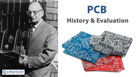
Paul Eisler and the Printed Circuit
In 1936, Austrian engineer Paul Eisler invented the printed circuit while working on a radio set. Eisler’s design involved printing conductive ink onto a non-conductive substrate, creating a more compact and efficient way to connect electronic components. Although Eisler’s idea was groundbreaking, it wasn’t until World War II that printed circuits gained significant attention.

The Role of PCBs in World War II
PCBs in Military Applications
During World War II, the demand for compact, reliable, and mass-producible electronic equipment skyrocketed. The U.S. military recognized the potential of printed circuits and began using them in various applications, such as proximity fuses for artillery shells and radio equipment for communication.
The Advent of the PCB Manufacturing Process
To meet the growing demand for printed circuits, the U.S. military collaborated with various companies to develop and refine the PCB manufacturing process. In 1943, the National Bureau of Standards (now known as the National Institute of Standards and Technology) published a report outlining the design and production of printed circuits, paving the way for standardization and mass production.

Post-War Advancements in PCB Technology
The Rise of Consumer Electronics
After World War II, the electronics industry shifted its focus to consumer products. The availability of reliable and affordable PCBs enabled the development of new consumer electronics, such as transistor radios, televisions, and early computers. As consumer demand grew, so did the need for more advanced PCB technologies.
The Introduction of Through-Hole Technology
In the 1950s, through-hole technology became the dominant method for mounting components on PCBs. This technology involved drilling holes in the PCB and inserting component leads through the holes, which were then soldered to the copper tracks on the other side of the board. Through-hole technology allowed for more complex circuit designs and improved reliability.
The Development of Surface Mount Technology (SMT)
As electronic devices became smaller and more sophisticated, through-hole technology began to reach its limitations. In the 1960s, surface mount technology (SMT) emerged as a solution to this problem. SMT involved placing components directly onto the surface of the PCB and soldering them in place, eliminating the need for drilled holes. This technology enabled the production of smaller, more densely packed PCBs.

The Digital Revolution and PCBs
The Impact of the Microprocessor
The invention of the microprocessor in the 1970s marked a turning point in the history of electronics. Microprocessors allowed for the development of more powerful and compact electronic devices, such as personal computers and mobile phones. As a result, PCBs had to evolve to accommodate these new, complex components.
The Rise of Multilayer PCBs
To cope with the increasing complexity of electronic circuits, multilayer PCBs were developed. These boards consisted of multiple layers of conductive material, separated by insulating layers, allowing for more intricate circuit designs and improved signal integrity. Multilayer PCBs became essential for high-speed digital applications, such as computers and telecommunications equipment.
The Advent of Computer-Aided Design (CAD)
The 1980s saw the widespread adoption of computer-aided design (CAD) tools in the PCB industry. CAD software allowed engineers to design and simulate PCBs digitally, streamlining the design process and reducing the risk of errors. This technology has continued to evolve, with modern CAD tools offering advanced features such as 3D modeling and automatic design rule checking.
Modern PCB Technologies and Applications
High-Density Interconnect (HDI) PCBs
As electronic devices continue to shrink in size and increase in functionality, high-density interconnect (HDI) PCBs have become increasingly popular. HDI PCBs feature finer traces, smaller vias, and higher component density than traditional PCBs, enabling the production of ultra-compact and high-performance electronic devices.
Flexible and Rigid-Flex PCBs
Flexible PCBs, made from flexible substrates such as polyimide, have gained traction in recent years due to their ability to conform to tight spaces and withstand repeated flexing. Rigid-flex PCBs, which combine rigid and flexible sections, offer the best of both worlds, providing the stability of traditional PCBs with the flexibility needed for certain applications, such as wearable electronics.
The Role of PCBs in the Internet of Things (IoT)
The proliferation of the Internet of Things (IoT) has created new opportunities and challenges for the PCB industry. IoT devices, which are often small, low-power, and wirelessly connected, require specialized PCBs that can accommodate these unique requirements. As the IoT continues to grow, the demand for innovative PCB solutions is expected to increase.
The Future of PCBs
Advanced Materials and Manufacturing Techniques
As the electronics industry continues to evolve, so too will the materials and manufacturing techniques used in PCB production. Researchers are exploring the use of advanced materials, such as graphene and carbon nanotubes, to create PCBs with improved thermal and electrical properties. Additionally, new manufacturing techniques, such as 3D printing and inkjet printing, are being developed to enable the production of more complex and customizable PCBs.
The Impact of Artificial Intelligence (AI) and Machine Learning (ML)
Artificial intelligence (AI) and machine learning (ML) are poised to revolutionize the PCB industry. These technologies can be used to optimize PCB designs, predict failures, and streamline manufacturing processes. As AI and ML continue to advance, we can expect to see more intelligent and efficient PCB solutions in the future.
The Importance of Sustainability in PCB Manufacturing
As environmental concerns continue to grow, the PCB industry is placing a greater emphasis on sustainability. This includes the development of eco-friendly materials, such as biodegradable substrates and lead-free solders, as well as the adoption of more sustainable manufacturing practices, such as energy-efficient equipment and waste reduction initiatives.
Frequently Asked Questions (FAQ)
-
Q: What is a printed circuit board (PCB)?
A: A printed circuit board (PCB) is a flat board made of insulating material with conductive pathways printed or etched onto its surface. PCBs are used to mechanically support and electrically connect electronic components. -
Q: Who invented the printed circuit board?
A: The concept of the printed circuit board can be traced back to the early 1900s, with German inventor Albert Hanson filing a patent for a device resembling a modern PCB in 1903. However, it was Austrian engineer Paul Eisler who invented the printed circuit as we know it today in 1936. -
Q: How did World War II impact the development of PCBs?
A: During World War II, the U.S. military recognized the potential of printed circuits and began using them in various applications, such as proximity fuses for artillery shells and radio equipment for communication. This increased demand led to the collaboration between the military and various companies to develop and refine the PCB manufacturing process. -
Q: What is the difference between through-hole technology and surface mount technology (SMT)?
A: Through-hole technology involves drilling holes in the PCB and inserting component leads through the holes, which are then soldered to the copper tracks on the other side of the board. In contrast, surface mount technology (SMT) involves placing components directly onto the surface of the PCB and soldering them in place, eliminating the need for drilled holes. -
Q: What role do PCBs play in the Internet of Things (IoT)?
A: IoT devices, which are often small, low-power, and wirelessly connected, require specialized PCBs that can accommodate these unique requirements. As the IoT continues to grow, the demand for innovative PCB solutions is expected to increase, driving the development of new PCB technologies and manufacturing techniques.
Conclusion
The history of printed circuit boards is a testament to human ingenuity and the relentless pursuit of technological advancement. From their humble beginnings in the early 20th century to their integral role in modern electronics, PCBs have undergone a remarkable evolution. As we look to the future, it is clear that PCBs will continue to shape the electronics industry, driven by advances in materials, manufacturing techniques, and emerging technologies such as AI and the IoT. By understanding the history of PCBs, we can better appreciate the challenges and opportunities that lie ahead, and work towards a more innovative and sustainable future for the electronics industry.


Leave a Reply