Introduction to Solder Stencils
Solder paste stencils are essential tools in the world of electronic assembly and printed circuit board (PCB) manufacturing. These thin, precision-cut sheets of metal or plastic are used to apply solder paste onto PCBs, ensuring accurate and consistent placement of solder for component attachment. In this comprehensive article, we will delve into the process of making solder paste stencils, exploring the materials, techniques, and best practices involved.
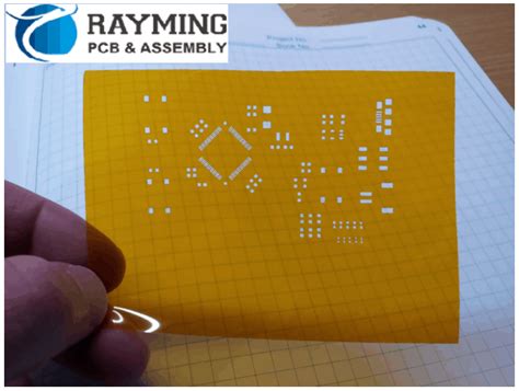
What are Solder Stencils?
Solder stencils are thin, flat sheets of material, typically stainless steel or polyester, that have precise openings or apertures corresponding to the pads on a PCB where solder paste needs to be applied. The stencil is placed over the PCB, and solder paste is spread across the surface using a squeegee or automated equipment. The paste flows through the openings, depositing the correct amount of solder onto the pads. This process ensures accurate and consistent solder paste application, which is crucial for achieving reliable solder joints during the reflow soldering process.
Importance of Solder Stencils in PCB Assembly
Solder stencils play a critical role in the PCB assembly process, particularly in surface mount technology (SMT). They offer several key benefits:
-
Precision: Solder stencils allow for precise control over the amount and placement of solder paste on PCB pads. This precision is essential for achieving reliable solder joints and preventing issues such as bridging or insufficient solder.
-
Consistency: By using a stencil, solder paste can be applied consistently across multiple PCBs, ensuring uniformity in the assembly process. This consistency is particularly important in high-volume production environments.
-
Efficiency: Solder stencils enable rapid and automated application of solder paste, significantly reducing the time and labor required compared to manual methods. This efficiency translates into faster production cycles and lower manufacturing costs.
-
Miniaturization: As electronic devices become smaller and more compact, the size of components and PCB features continues to shrink. Solder stencils allow for the precise application of solder paste on these tiny pads, enabling the assembly of miniaturized components and high-density PCB designs.
Materials Used for Solder Stencils
Solder stencils can be made from various materials, each with its own advantages and limitations. The choice of material depends on factors such as durability, precision requirements, cost, and the specific application. Let’s explore the common materials used for solder stencils:
Stainless Steel Stencils
Stainless steel is the most widely used material for solder stencils due to its durability, precision, and long lifespan. Stainless steel stencils are typically made from high-quality, fine-grain stainless steel sheets with a thickness ranging from 0.1mm to 0.2mm (4 to 8 mils). The apertures in the stencil are created using laser cutting or chemical etching processes, ensuring high accuracy and clean edges.
Advantages of stainless steel stencils include:
– Excellent durability and resistance to wear and tear
– High precision and sharp aperture edges
– Suitable for high-volume production and repeated use
– Compatible with various solder paste types and cleaning methods
Disadvantages of stainless steel stencils include:
– Higher cost compared to other materials
– Requires specialized equipment for cutting and handling
– Can be prone to warping or damage if not handled properly
Polyester Stencils
Polyester stencils, also known as mesh stencils or screen stencils, are made from a thin, flexible polyester film. The apertures in the stencil are created by printing a pattern onto the film using a high-resolution photographic process. Polyester stencils are commonly used for prototyping, low-volume production, and applications where flexibility and low cost are desired.
Advantages of polyester stencils include:
– Lower cost compared to stainless steel stencils
– Flexibility and ease of handling
– Suitable for quick prototyping and low-volume production
– Can be easily cut and modified as needed
Disadvantages of polyester stencils include:
– Lower durability compared to stainless steel stencils
– Reduced precision and aperture quality
– Limited compatibility with certain solder paste types
– May stretch or deform over time, affecting print quality
Other Materials
While stainless steel and polyester are the most common materials for solder stencils, other materials may be used in specific applications:
-
Nickel Stencils: Nickel stencils offer high durability and corrosion resistance, making them suitable for harsh environments or applications with aggressive solder paste formulations.
-
Titanium Stencils: Titanium stencils provide excellent strength and durability, but they are more expensive than stainless steel and are typically used in specialized applications.
-
Plastic Stencils: Plastic stencils, such as those made from acrylic or polycarbonate, are sometimes used for low-cost, disposable applications or in situations where a non-conductive stencil is required.
| Material | Durability | Precision | Cost | Typical Thickness |
|---|---|---|---|---|
| Stainless Steel | High | High | High | 0.1mm – 0.2mm |
| Polyester | Low | Moderate | Low | 0.1mm – 0.15mm |
| Nickel | High | High | High | 0.1mm – 0.2mm |
| Titanium | Very High | High | Very High | 0.1mm – 0.2mm |
| Plastic | Low | Low | Low | 0.1mm – 0.3mm |

Solder Stencil Manufacturing Process
The manufacturing process for solder stencils involves several key steps, from design and artwork preparation to the actual cutting or etching of the stencil. Let’s explore each step in detail:
Step 1: Stencil Design and Artwork Preparation
The first step in making a solder stencil is to create the stencil design based on the PCB layout. This involves generating a stencil artwork file, typically in Gerber format, which contains the precise dimensions and locations of the apertures corresponding to the solder pads on the PCB.
The stencil artwork is created using PCB design software or specialized stencil design tools. The artwork must take into account factors such as aperture size, shape, and pitch, as well as any specific requirements for fine-pitch components or unique pad geometries.
Step 2: Material Selection and Preparation
Once the stencil artwork is ready, the next step is to select the appropriate material for the stencil based on the specific requirements of the application. As discussed earlier, stainless steel and polyester are the most common choices, but other materials like nickel or titanium may be used in specialized cases.
The selected material is then prepared for the cutting or etching process. For stainless steel stencils, the sheet is typically cleaned and inspected for any defects or irregularities. Polyester stencils may require additional preparation steps, such as applying a photosensitive coating or laminating the film to a rigid backing material.
Step 3: Stencil Cutting or Etching
The actual process of creating the apertures in the stencil differs depending on the material and manufacturing method used. The two most common methods are laser cutting and chemical etching.
Laser Cutting
Laser cutting is the preferred method for creating stainless steel stencils. A high-precision laser beam is used to cut the apertures into the stainless steel sheet according to the stencil artwork. The laser beam vaporizes the metal, creating clean and precise openings with smooth edges.
Advantages of laser cutting include:
– High precision and accuracy
– Clean and burr-free aperture edges
– Fast and efficient cutting process
– Suitable for complex aperture shapes and fine-pitch designs
Disadvantages of laser cutting include:
– Higher equipment and operating costs
– Potential for heat-affected zones around apertures
– Limited material thickness range
Chemical Etching
Chemical etching is commonly used for creating polyester stencils and can also be used for stainless steel stencils in some cases. In this process, the stencil material is coated with a photoresist layer, and the stencil artwork is used to expose and develop the pattern on the photoresist. The exposed areas are then chemically etched away, leaving the desired apertures in the stencil.
Advantages of chemical etching include:
– Lower equipment and operating costs compared to laser cutting
– Suitable for larger apertures and simpler designs
– Can be used with a wider range of materials, including polyester and stainless steel
Disadvantages of chemical etching include:
– Lower precision compared to laser cutting
– Potential for undercutting and less clean aperture edges
– Slower process compared to laser cutting
– Environmental and safety concerns related to the use of chemicals
Step 4: Cleaning and Inspection
After the stencil has been cut or etched, it undergoes a thorough cleaning process to remove any debris, residues, or contaminants. This typically involves using specialized cleaning agents and ultrasonic cleaning equipment to ensure a clean and pristine stencil surface.
Once cleaned, the stencil is inspected for accuracy and quality. This may involve using optical inspection systems or microscopes to verify aperture dimensions, position, and edge quality. Any defects or deviations from the stencil artwork are identified and corrected if necessary.
Step 5: Packaging and Delivery
The final step in the solder stencil manufacturing process is packaging and delivery. The stencil is typically packaged in a protective sleeve or container to prevent damage during transport and storage. Proper labeling and identification are applied to the package, including the stencil specifications, material type, and any customer-specific information.
The packaged stencil is then shipped to the customer or end-user, ready for use in the PCB assembly process.

Solder Stencil Design Considerations
Designing an effective solder stencil involves several key considerations to ensure optimal solder paste deposition and PCB assembly results. Let’s explore some of the critical design factors:
Aperture Size and Shape
The size and shape of the apertures in the solder stencil have a significant impact on the amount and distribution of solder paste deposited on the PCB pads. The aperture dimensions must be carefully calculated based on the pad size, component pitch, and solder paste rheology.
-
Aperture Width: The width of the aperture should be slightly larger than the width of the PCB pad to allow for proper solder paste release. A typical guideline is to add 10-20% to the pad width for the aperture width.
-
Aperture Length: The length of the aperture should be long enough to accommodate the desired volume of solder paste while considering the stencil thickness. A common rule of thumb is to use an aspect ratio (length to width) of 1.5 to 2.0 for optimal paste release.
-
Aperture Shape: The shape of the aperture can affect the solder paste deposition and release characteristics. Common aperture shapes include rectangular, rounded rectangular, and home plate (trapezoidal). The choice of shape depends on factors such as pad geometry, component type, and solder paste properties.
Stencil Thickness
The thickness of the solder stencil determines the volume of solder paste deposited on the PCB pads. Choosing the appropriate stencil thickness is crucial for achieving the desired solder joint quality and preventing defects such as bridging or insufficient solder.
Typical stencil thicknesses range from 0.1mm to 0.2mm (4 to 8 mils), depending on the specific requirements of the PCB design and components. Factors to consider when selecting stencil thickness include:
- Component pitch and size
- Solder paste type and properties
- PCB Surface Finish and pad geometry
- Manufacturing process capabilities
Thinner stencils (0.1mm to 0.15mm) are generally used for fine-pitch components and high-density PCB designs, while thicker stencils (0.15mm to 0.2mm) are suitable for larger components and standard pitch designs.
Aperture Orientation and Positioning
The orientation and positioning of the apertures in the stencil should match the placement of the pads on the PCB. Proper alignment is critical to ensure accurate solder paste deposition and prevent issues such as bridging or misaligned components.
-
Aperture Orientation: The apertures should be oriented to match the orientation of the pads on the PCB. This is particularly important for components with rectangular or elongated pads, such as chip resistors or capacitors.
-
Aperture Positioning: The position of the apertures should be precisely aligned with the corresponding pads on the PCB. Any misalignment can lead to solder paste deposition in the wrong location or insufficient coverage of the pads.
To ensure accurate aperture positioning, the stencil artwork must be carefully created and reviewed against the PCB layout. Alignment marks or fiducials can be included in the stencil design to aid in the alignment process during stencil printing.
Stencil Escapes and Reliefs
Stencil escapes and reliefs are design features that help improve solder paste release and prevent issues such as bridging or solder paste smearing.
-
Escapes: Escapes are small extensions or openings added to the apertures to provide a path for excess solder paste to flow away from the main aperture. They help prevent bridging between adjacent pads and improve solder paste release.
-
Reliefs: Reliefs are larger openings or cutouts in the stencil that allow for solder paste to be deposited in areas away from the main apertures. They are typically used for large component pads or in areas where additional solder paste volume is required.
Incorporating escapes and reliefs into the stencil design can help optimize solder paste deposition and improve the overall quality of the solder joints.
Stencil Fiducials and Markings
Fiducials and markings are additional features included in the stencil design to aid in alignment, identification, and quality control.
-
Fiducials: Fiducials are precise reference marks placed on the stencil that correspond to specific locations on the PCB. They are used for aligning the stencil to the PCB during the printing process, ensuring accurate solder paste deposition. Fiducials are typically placed in the corners or edges of the stencil and PCB.
-
Markings: Markings are text or symbols added to the stencil for identification and traceability purposes. They may include information such as the stencil version, material type, thickness, or customer-specific data. Markings help ensure the correct stencil is used for the corresponding PCB and provide a reference for quality control and troubleshooting.
Including fiducials and markings in the stencil design helps streamline the assembly process, improve alignment accuracy, and facilitate traceability and quality control.

Solder Stencil Printing Process
Once the solder stencil has been manufactured and the PCB is ready for assembly, the solder stencil printing process can begin. This process involves applying solder paste to the PCB pads through the apertures in the stencil. Let’s explore the key steps involved in solder stencil printing:
Step 1: Stencil and PCB Alignment
The first step in the printing process is to align the solder stencil with the PCB. This is typically done using a stencil printer, which is a specialized machine designed for precise stencil-to-PCB alignment and solder paste deposition.
The PCB is placed on the printer’s substrate carrier, and the solder stencil is positioned above the PCB. The alignment is achieved using the fiducials on the stencil and PCB, which are recognized by the printer’s vision system. The printer adjusts the position of the stencil or PCB until the fiducials are perfectly aligned.
Step 2: Solder Paste Application
Once the stencil and PCB are aligned, the solder paste is applied to the stencil surface. This is typically done using a solder paste dispenser or a manual applicator.
The solder paste is placed on one end of the stencil and then spread across the surface using a squeegee blade. The blade is moved across the stencil at a controlled speed and pressure, forcing the solder paste through the apertures and onto the PCB pads.
The quality of the solder paste deposition depends on several factors, including:
– Solder paste properties (viscosity, particle size, etc.)
– Squeegee blade material and shape
– Print speed and pressure
– Stencil aperture design and surface finish
Step 3: Stencil Separation
After the solder paste has been deposited onto the PCB pads, the stencil is carefully separated from the PCB. This is done by slowly lifting the stencil away from the PCB surface, allowing the solder paste to release from the apertures and remain on the pads.
Proper stencil separation is critical to ensuring a clean and consistent solder paste print. Factors such as stencil-to-PCB gap, separation speed, and stencil surface finish can affect the quality of the solder paste release.
Step 4: Inspection and Touch-up
Once


Leave a Reply