Introduction to PCB Manufacturing
Printed Circuit Boards (PCBs) are the backbone of modern electronics. They provide a platform for electrical components to be mounted and connected, enabling the creation of complex circuits in a compact and organized manner. PCB manufacturing is a multi-step process that involves various techniques and technologies to produce high-quality, reliable boards. In this article, we will delve into the step-by-step process of PCB manufacturing, from design to final assembly.
PCB Design and Preparation
PCB Design Software
The first step in PCB manufacturing is the design phase. Engineers use specialized PCB design software, such as Altium Designer, EAGLE, or KiCad, to create the schematic and layout of the circuit board. These software tools allow designers to place components, route traces, and define the board’s dimensions and features.
Design Considerations
When designing a PCB, several factors must be considered to ensure optimal performance and manufacturability:
- Component placement: Components should be placed in a logical and efficient manner, taking into account signal integrity, heat dissipation, and mechanical constraints.
- Trace routing: Traces should be routed to minimize signal interference, maintain appropriate trace widths and spacings, and avoid sharp angles that can cause manufacturing issues.
- Layer stack-up: The number and arrangement of copper layers in the PCB should be determined based on the complexity of the circuit and the required signal integrity.
- Design for manufacturing (DFM): The design should adhere to manufacturing guidelines, such as minimum trace widths, hole sizes, and clearances, to ensure the board can be reliably produced.
Gerber File Generation
Once the PCB design is complete, the designer generates a set of Gerber files, which are the industry-standard format for describing the layout of a PCB. Gerber files contain information about each layer of the board, including copper traces, solder mask, silkscreen, and drill holes. These files are sent to the PCB manufacturer for production.

PCB Fabrication Process
Step 1: Copper Clad Laminate Preparation
The PCB fabrication process begins with the preparation of the copper clad laminate (CCL). CCL is a substrate material, typically made of fiberglass (FR-4) or other dielectric materials, with a thin layer of copper foil bonded to one or both sides. The copper foil thickness can vary depending on the application, with common thicknesses being 0.5 oz (18 µm), 1 oz (35 µm), and 2 oz (70 µm).
The CCL is cut to the desired size using a high-precision cutting machine, such as a CNC router or a laser cutter. The cutting process ensures that the board dimensions are accurate and consistent.
Step 2: Drilling
After the CCL is cut to size, the next step is drilling. Holes are drilled into the board to accommodate through-hole components, vias (vertical interconnect access), and mounting holes. The drilling process is performed using high-speed, computer-controlled drill machines that can produce holes with diameters as small as 0.1 mm.
The drill machine uses a drill file, which is generated from the PCB design software, to determine the location and size of each hole. The drill file is typically in the Excellon format, which is an industry-standard for describing drill data.
Step 3: Copper Patterning
With the holes drilled, the next step is to create the copper patterns on the board. There are two primary methods for copper patterning: subtractive and additive.
Subtractive Method
The subtractive method, also known as etching, involves removing unwanted copper from the CCL to create the desired circuit pattern. The process begins by applying a photoresist layer to the copper surface. The photoresist is a light-sensitive material that hardens when exposed to ultraviolet (UV) light.
A photomask, which is a film containing the circuit pattern, is placed on top of the photoresist, and the board is exposed to UV light. The areas of the photoresist that are not covered by the photomask harden, while the areas that are covered remain soluble.
The board is then developed in a chemical solution that removes the soluble photoresist, exposing the underlying copper. The exposed copper is etched away using a chemical etchant, typically ferric chloride or ammonium persulfate, leaving behind the desired circuit pattern.
Additive Method
The additive method, also known as plating, involves adding copper to the board to create the circuit pattern. This method is less common than the subtractive method but is gaining popularity due to its ability to produce finer features and higher-density circuits.
One additive method is called the semi-additive process (SAP). In this process, a thin layer of copper is electrolessly plated onto the entire surface of the board. A photoresist is then applied and patterned using a photomask, similar to the subtractive method.
The exposed areas of the thin copper layer are then electroplated with additional copper, building up the thickness of the traces. The photoresist is removed, and the thin copper layer is etched away, leaving behind the plated copper traces.
Step 4: Solder Mask Application
After the copper patterning is complete, a solder mask is applied to the board. The solder mask is a protective layer that covers the copper traces, leaving only the areas intended for soldering exposed. The solder mask serves several purposes:
- Insulates the copper traces from accidental short circuits
- Protects the copper from oxidation and corrosion
- Provides a surface for silkscreen printing
- Improves the aesthetics of the board
The solder mask is typically applied using a screen printing process or a photoimageable process similar to the one used for copper patterning.
Step 5: Silkscreen Printing
Silkscreen printing is the process of adding text, logos, and other identifying marks to the PCB. The silkscreen is usually printed on top of the solder mask using a screen printing process. The ink used for silkscreen printing is typically white, but other colors are available.
The silkscreen provides important information for assembly and troubleshooting, such as component designators, polarity markers, and test points.
Step 6: Surface Finish
The final step in the PCB fabrication process is the application of a surface finish. The surface finish is a thin layer of metal applied to the exposed copper areas of the board, such as pads and through-holes. The surface finish serves several purposes:
- Protects the copper from oxidation and corrosion
- Enhances the solderability of the pads
- Improves the electrical and mechanical reliability of the solder joints
There are several types of surface finishes available, each with its own advantages and disadvantages:
| Surface Finish | Advantages | Disadvantages |
|---|---|---|
| HASL (Hot Air Solder Leveling) | – Low cost – Good solderability – Widely available |
– Uneven surface – Not suitable for fine-pitch components |
| ENIG (Electroless Nickel Immersion Gold) | – Flat surface – Excellent solderability – Suitable for fine-pitch components |
– Higher cost than HASL – Nickel corrosion in some environments |
| OSP (Organic Solderability Preservative) | – Low cost – Flat surface – Suitable for fine-pitch components |
– Limited shelf life – Not suitable for multiple reflow cycles |
| Immersion Silver | – Low cost – Flat surface – Good solderability |
– Limited shelf life – Can tarnish over time |
| Immersion Tin | – Low cost – Flat surface – Good solderability |
– Limited shelf life – Tin whiskers can cause short circuits |
The choice of surface finish depends on the specific requirements of the application, such as cost, solderability, shelf life, and compatibility with the assembly process.

PCB Assembly
After the PCB fabrication process is complete, the board is ready for assembly. PCB assembly involves the placement and soldering of components onto the board.
Step 1: Solder Paste Application
The first step in PCB assembly is the application of solder paste to the pads on the board. Solder paste is a mixture of tiny solder particles suspended in a flux matrix. The solder paste is applied using a stencil printing process, where a stainless steel stencil with openings corresponding to the pads is placed over the board, and the solder paste is spread across the stencil using a squeegee.
The stencil ensures that the solder paste is applied in the correct locations and in the right amount. The thickness of the stencil and the size of the openings determine the volume of solder paste applied to each pad.
Step 2: Component Placement
After the solder paste is applied, the components are placed onto the board. For through-hole components, the leads are inserted into the corresponding holes in the board. For surface-mount components, the components are placed onto the pads with the solder paste.
Component placement can be done manually for low-volume production or prototypes, but for high-volume production, automated pick-and-place machines are used. These machines use computer vision and precision robotics to pick up components from reels or trays and place them onto the board with high speed and accuracy.
Step 3: Reflow Soldering
After the components are placed, the board undergoes a reflow soldering process. In reflow soldering, the board is heated in a controlled manner to melt the solder paste and form a permanent electrical and mechanical connection between the components and the pads.
The reflow soldering process typically follows a temperature profile that includes several stages:
- Preheat: The board is gradually heated to activate the flux and remove any moisture from the components and the board.
- Soak: The board is held at a stable temperature to allow the flux to clean the surfaces of the pads and the component leads.
- Reflow: The temperature is rapidly increased to melt the solder particles and form a solder joint between the components and the pads.
- Cooling: The board is cooled down gradually to allow the solder joints to solidify and prevent thermal shock to the components.
The temperature profile is carefully controlled to ensure that the solder joints are formed correctly and to prevent damage to the components or the board.
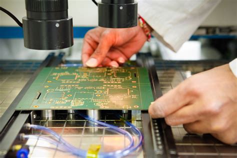
Step 4: Inspection and Testing
After the reflow soldering process, the board undergoes inspection and testing to ensure that it meets the required quality standards. Visual inspection is performed to check for any visible defects, such as misaligned components, solder bridges, or insufficient solder joints.
Automated optical inspection (AOI) machines can be used to quickly scan the board and detect any defects that may be difficult to see with the naked eye. AOI machines use high-resolution cameras and advanced image processing algorithms to compare the assembled board to a reference image and identify any discrepancies.
Electrical testing is also performed to verify that the board functions as intended. This can include in-circuit testing (ICT), where a test fixture is used to make electrical contact with specific points on the board and measure the electrical characteristics of the components and the connections. Functional testing may also be performed to validate the overall performance of the board in its intended application.
Step 5: Conformal Coating and Potting
In some applications, the assembled PCB may require additional protection from environmental factors, such as moisture, dust, or chemicals. Conformal coating and potting are two methods used to provide this protection.
Conformal coating involves applying a thin layer of a protective material, such as acrylic, silicone, or polyurethane, over the surface of the board and the components. The coating helps to seal the board and prevent moisture and contaminants from reaching the components and the connections.
Potting involves encapsulating the board and the components in a solid material, such as epoxy or silicone. Potting provides a higher level of protection than conformal coating but can also make the board more difficult to repair or modify.

Quality Control and Standards
To ensure the reliability and consistency of PCBs, manufacturers follow various quality control procedures and adhere to industry standards.
IPC Standards
The Association Connecting Electronics Industries (IPC) is a global trade association that develops and maintains standards for the electronic interconnect industry. IPC standards cover various aspects of PCB design, fabrication, and assembly, including:
- IPC-A-600: Acceptability of Printed Boards
- IPC-A-610: Acceptability of Electronic Assemblies
- IPC-6012: Qualification and Performance Specification for Rigid Printed Boards
- IPC-J-STD-001: Requirements for Soldered Electrical and Electronic Assemblies
These standards provide guidelines and criteria for evaluating the quality and reliability of PCBs and assemblies.
ISO Standards
The International Organization for Standardization (ISO) also has standards that apply to the PCB industry, such as:
- ISO 9001: Quality Management Systems
- ISO 14001: Environmental Management Systems
- ISO 45001: Occupational Health and Safety Management Systems
Adhering to these standards helps PCB manufacturers ensure consistent quality, minimize environmental impact, and maintain a safe working environment.
Testing and Inspection
In addition to the inspection and testing performed during the assembly process, PCBs may undergo additional testing to validate their performance and reliability. Some common tests include:
- Environmental testing: Exposing the board to various environmental conditions, such as temperature cycling, humidity, and vibration, to ensure that it can withstand the intended operating conditions.
- Accelerated life testing: Subjecting the board to elevated stress levels to simulate long-term use and identify potential failure modes.
- Functional testing: Verifying that the board performs its intended functions and meets the specified performance requirements.
Frequently Asked Questions (FAQ)
- What is the difference between a single-sided and a double-sided PCB?
-
A single-sided PCB has copper traces and components on only one side of the board, while a double-sided PCB has copper traces and components on both sides of the board. Double-sided PCBs offer more design flexibility and higher component density but are more complex to manufacture.
-
What is the purpose of vias in a PCB?
-
Vias are small holes drilled through the PCB that allow electrical connections to be made between different layers of the board. They are used to route signals between layers and to connect components on opposite sides of the board.
-
What is the difference between through-hole and surface-mount components?
-
Through-hole components have leads that are inserted into holes drilled in the PCB and soldered to pads on the opposite side of the board. Surface-mount components are placed directly onto pads on the surface of the board and soldered in place. Surface-mount components are smaller and allow for higher component density, but they require more precise placement and soldering.
-
What is the purpose of the solder mask on a PCB?
-
The solder mask is a protective layer that covers the copper traces on the PCB, leaving only the areas intended for soldering exposed. It helps to prevent accidental short circuits, protects the copper from oxidation and corrosion, and provides a surface for silkscreen printing.
-
What is the difference between reflow soldering and wave soldering?
- Reflow soldering is used for surface-mount components and involves applying solder paste to the pads, placing the components, and then heating the board to melt the solder and form the solder joints. Wave soldering is used for through-hole components and involves passing the board over a wave of molten solder, which flows into the holes and forms the solder joints.
Conclusion
PCB manufacturing is a complex process that involves multiple steps and technologies to produce high-quality, reliable boards. From design and preparation to fabrication and assembly, each step plays a critical role in ensuring the functionality and durability of the final product.
By understanding the PCB manufacturing process and adhering to industry standards and best practices, designers and manufacturers can create PCBs that meet the demanding requirements of modern electronics applications. As technology continues to advance, the PCB industry will continue to evolve and innovate to support the development of ever-more complex and sophisticated electronic devices.


Leave a Reply