Key Features of PCB Visualizer
PCB Visualizer offers a range of features that make it an essential tool for PCB design:
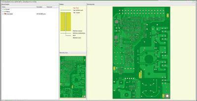
1. 3D Visualization
The primary feature of PCB Visualizer is its ability to render PCB designs in realistic 3D. This allows designers to:
- View the board from any angle
- Examine component placement and orientation
- Check for clearance issues between components
- Ensure proper fitting of the PCB in its enclosure
2. Real-Time Design Updates
PCB Visualizer integrates with popular PCB design software, enabling real-time updates to the 3D model as the design is modified. This means that any changes made to the PCB layout are immediately reflected in the 3D visualization, providing instant feedback to the designer.
3. Component Libraries
PCB Visualizer includes extensive libraries of 3D models for common electronic components. These libraries cover a wide range of component types, including:
| Component Type | Examples |
|---|---|
| Resistors | Surface mount, through-hole |
| Capacitors | Ceramic, electrolytic, tantalum |
| Inductors | Surface mount, through-hole |
| Diodes | Signal, rectifier, Zener |
| Transistors | Bipolar, MOSFET |
| Integrated Circuits | SOICs, QFPs, BGAs |
| Connectors | Pin headers, USB, HDMI |
Designers can also import custom 3D models for components not included in the libraries.
4. Design Rule Checking (DRC)
PCB Visualizer can perform automated design rule checks to identify potential issues in the PCB layout. This includes checking for:
- Minimum clearance between components
- Proper pad sizes for component footprints
- Sufficient spacing between traces
- Compliance with manufacturing constraints
By catching these issues early, designers can avoid costly redesigns and manufacturing delays.
5. Collaboration and Sharing
PCB Visualizer supports collaboration among design team members by allowing them to share 3D models and design data. This enables:
- Design reviews and feedback
- Collaboration between electrical and mechanical engineers
- Sharing of design files with manufacturers
Benefits of Using PCB Visualizer
Using PCB Visualizer in the PCB design process offers several key benefits:
-
Improved Design Quality: By providing a realistic 3D representation of the PCB, Visualizer helps designers identify and correct issues that may not be apparent in a 2D layout. This leads to higher quality designs with fewer errors.
-
Faster Design Iterations: With real-time updates and automated design rule checking, designers can quickly make changes to the PCB layout and receive instant feedback. This speeds up the design process and allows for more iterations in less time.
-
Better Communication: 3D visualizations are easier to understand than 2D layouts, especially for non-technical stakeholders. PCB Visualizer makes it easier to communicate design intent and get buy-in from other team members and project stakeholders.
-
Reduced Manufacturing Issues: By identifying potential manufacturing issues early in the design process, PCB Visualizer helps avoid costly redesigns and delays. This results in smoother manufacturing runs and faster time-to-market.

PCB Visualizer Workflow
The typical workflow for using PCB Visualizer involves the following steps:
-
Design Creation: The PCB layout is created using a compatible PCB design software, such as Altium Designer or KiCad.
-
3D Model Generation: PCB Visualizer automatically generates a 3D model of the PCB based on the design files. This model includes the board substrate, copper traces, and 3D models of the components.
-
Design Review: The designer can now view the PCB from any angle, zoom in on specific areas, and check for potential issues. Design rule checks can be run to identify any violations of manufacturing constraints.
-
Collaboration: The 3D model can be shared with other team members for review and feedback. Mechanical engineers can use the model to ensure proper fitting of the PCB in the enclosure.
-
Design Refinement: Based on the feedback and insights gained from the 3D visualization, the designer can make necessary changes to the PCB layout. These changes are instantly reflected in the 3D model.
-
Manufacturing Preparation: Once the design is finalized, PCB Visualizer can generate manufacturing files, such as Gerber files and drill files, that can be sent to the PCB manufacturer.

Case Studies
Several companies have successfully used PCB Visualizer to improve their PCB design process:
Company A: Consumer Electronics
Company A designs and manufactures consumer electronics products. By adopting PCB Visualizer, they were able to:
- Reduce the number of design iterations by 30%
- Identify and correct 95% of design issues before sending files to manufacturing
- Improve communication between electrical and mechanical engineering teams
- Shorten overall product development time by 20%
Company B: Automotive Electronics
Company B specializes in automotive electronics, where reliability and safety are critical. PCB Visualizer helped them:
- Ensure proper component placement and orientation for vibration resistance
- Verify adequate clearance between high-voltage components
- Optimize board layout for efficient heat dissipation
- Achieve first-pass success in manufacturing for 90% of their designs

FAQ
- What PCB design software is compatible with PCB Visualizer?
PCB Visualizer is compatible with popular PCB design software, including:
– Altium Designer
– KiCad
– Cadence Allegro
– Mentor Graphics PADS
– Eagle
- Can I import custom 3D models into PCB Visualizer?
Yes, PCB Visualizer allows you to import custom 3D models in common formats such as STEP, IGES, and OBJ. This is useful for components that are not included in the standard libraries.
- Does PCB Visualizer support multi-board designs?
Yes, PCB Visualizer can handle multi-board designs, allowing you to visualize how multiple PCBs fit together in an assembly.
- Can I export the 3D model from PCB Visualizer for use in other software?
PCB Visualizer allows you to export the 3D model in various formats, such as STEP, IGES, and OBJ, for use in mechanical design software or for 3D printing.
- Is there a learning curve for using PCB Visualizer?
PCB Visualizer is designed to be intuitive and user-friendly. Most designers familiar with PCB design software can start using PCB Visualizer effectively within a few hours. The software also includes comprehensive documentation and tutorials to help users get up to speed quickly.
Conclusion
PCB Visualizer is a powerful tool that is transforming the way PCBs are designed and manufactured. By providing realistic 3D visualizations, real-time design updates, and automated design rule checking, PCB Visualizer helps designers create higher quality PCBs in less time. As PCB complexity continues to increase, tools like PCB Visualizer will become increasingly essential for electronics companies looking to stay competitive in today’s fast-paced market.


Leave a Reply