What is PCB Inspection?
PCB inspection is the process of examining a printed circuit board for defects, anomalies, and compliance with design specifications. The goal of PCB inspection is to identify and correct any issues before the board is assembled into a final product.
PCB inspection can be performed at various stages of the manufacturing process, including:
- Pre-production inspection: This involves checking the PCB design files, Gerber files, and bill of materials (BOM) for accuracy and completeness before production begins.
- In-process inspection: This involves inspecting the PCB at various points during the manufacturing process, such as after solder paste application, component placement, and reflow soldering.
- Post-production inspection: This involves a final inspection of the completed PCB to ensure that it meets all quality standards and functional requirements.
Common PCB Defects
There are many types of defects that can occur during PCB manufacturing. Some of the most common include:
Solder Defects
Solder defects are among the most common types of PCB defects. They can occur due to issues with solder paste application, component placement, or reflow soldering. Some common solder defects include:
| Defect | Description |
|---|---|
| Bridging | Solder connecting two or more pins or pads that should not be connected |
| Insufficient solder | Not enough solder to create a reliable connection |
| Tombstoning | One end of a component lifts off the pad due to uneven heating or surface tension |
| Solder balls | Small balls of solder that can cause short circuits |
Component Defects
Component defects can occur due to issues with the components themselves or with their placement on the PCB. Some common component defects include:
| Defect | Description |
|---|---|
| Missing components | Components that are missing from the PCB |
| Misaligned components | Components that are not placed accurately on their pads |
| Damaged components | Components that are cracked, bent, or otherwise damaged |
| Incorrect components | Components that do not match the BOM or design specifications |
Circuit Defects
Circuit defects are issues with the copper traces and vias on the PCB. Some common circuit defects include:
| Defect | Description |
|---|---|
| Open circuits | Broken or incomplete traces that prevent electrical continuity |
| Short circuits | Unintended connections between traces or components |
| Underetch | Traces that are too narrow due to insufficient etching |
| Overetch | Traces that are too wide due to excessive etching |

PCB Inspection Methods
There are several methods used for PCB inspection, ranging from visual inspection to automated optical inspection (AOI) and X-ray inspection. Let’s take a closer look at each of these methods.
Visual Inspection
Visual inspection is the most basic form of PCB inspection. It involves examining the PCB with the naked eye or with the aid of a magnifying glass or microscope. Visual inspection can detect obvious defects such as missing components, solder bridges, or damaged boards.
However, visual inspection has several limitations:
- It is time-consuming and labor-intensive
- It is subjective and prone to human error
- It cannot detect hidden or subsurface defects
Despite these limitations, visual inspection is still an important part of the PCB inspection process, particularly for low-volume or prototype builds.
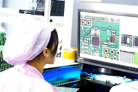
Automated Optical Inspection (AOI)
Automated optical inspection (AOI) is a more advanced form of PCB inspection that uses cameras and image processing software to detect defects. AOI systems can scan the entire PCB surface in a matter of seconds and compare the images to a reference image or CAD file.
AOI systems can detect a wide range of defects, including:
- Solder defects (bridging, insufficient solder, tombstoning, etc.)
- Component defects (missing, misaligned, or damaged components)
- Circuit defects (open or short circuits, underetch, overetch)
- Foreign material or debris on the board
AOI systems offer several advantages over manual inspection:
- They are faster and more efficient
- They are more consistent and repeatable
- They can detect smaller and more subtle defects
However, AOI systems also have some limitations:
- They can only detect surface defects, not hidden or subsurface issues
- They require a reference image or CAD file for comparison
- They can generate false positives or false negatives if not properly calibrated or programmed
X-Ray Inspection
X-ray inspection is a specialized form of PCB inspection that uses X-rays to penetrate the board and detect defects that are not visible on the surface. X-ray inspection is particularly useful for inspecting:
- Ball grid array (BGA) and chip scale package (CSP) components
- Flip-chip and package-on-package (PoP) assemblies
- Vias and plated through-holes
- Solder joints under components
X-ray inspection systems use either 2D or 3D imaging techniques to create detailed images of the internal structure of the PCB. These images can be analyzed by software algorithms to detect defects such as:
- Voids or cracks in solder joints
- Misaligned or missing balls in BGA components
- Broken or incomplete vias
- Foreign material or debris inside the board
X-ray inspection offers several advantages over other inspection methods:
- It can detect hidden or subsurface defects
- It can image complex assemblies and high-density boards
- It is non-destructive and does not require physical contact with the board
However, X-ray inspection also has some limitations:
- It requires specialized equipment and trained operators
- It can be slower and more expensive than other inspection methods
- It can generate false positives or false negatives if not properly calibrated or interpreted

Best Practices for PCB Inspection
To ensure effective and efficient PCB inspection, it is important to follow some best practices:
-
Develop a comprehensive inspection plan: Define the inspection criteria, methods, and acceptance standards for each stage of the manufacturing process.
-
Use a combination of inspection methods: No single inspection method can catch all defects. Use a combination of visual, AOI, and X-ray inspection as appropriate for the complexity and criticality of the PCB.
-
Calibrate and maintain inspection equipment: Ensure that all inspection equipment is properly calibrated and maintained to ensure accurate and consistent results.
-
Train and certify inspection personnel: Provide adequate training and certification for inspection personnel to ensure that they have the knowledge and skills to perform effective inspections.
-
Document and analyze inspection results: Record and analyze inspection results to identify trends, root causes, and opportunities for improvement.
-
Continuously improve the inspection process: Use data and feedback from inspections to continuously improve the design, manufacturing, and inspection processes.

FAQ
What is the difference between AOI and visual inspection?
AOI uses automated cameras and software to scan the PCB surface and detect defects, while visual inspection relies on human vision and judgment. AOI is faster, more consistent, and can detect smaller defects than visual inspection, but it can only detect surface defects and requires a reference image or CAD file for comparison.
Can X-ray inspection detect all types of defects?
No, X-ray inspection is best suited for detecting hidden or subsurface defects, such as voids or cracks in solder joints, misaligned or missing balls in BGA components, and broken or incomplete vias. It may not be able to detect surface defects or anomalies that are not visible in the X-ray image.
How often should PCB inspection be performed?
PCB inspection should be performed at various stages of the manufacturing process, including pre-production, in-process, and post-production. The frequency and scope of inspection will depend on the complexity and criticality of the PCB, as well as the quality and reliability requirements of the end product.
What are the acceptance criteria for PCB inspection?
The acceptance criteria for PCB inspection will vary depending on the specific application and industry standards. In general, PCBs should be free of defects that could affect the functionality, reliability, or safety of the end product. Some common acceptance criteria include:
- No solder defects such as bridging, insufficient solder, or tombstoning
- All components present, properly oriented, and undamaged
- No open or short circuits
- Trace width and spacing within specifications
- No foreign material or debris on the board
Can PCB inspection guarantee 100% defect-free boards?
No, PCB inspection cannot guarantee 100% defect-free boards, as there is always a possibility of human error, equipment malfunction, or other variables that can introduce defects. However, effective PCB inspection can significantly reduce the likelihood of defects and ensure that the vast majority of boards meet quality and reliability standards.
Conclusion
PCB inspection is a critical step in the manufacturing process that helps ensure the quality, reliability, and functionality of printed circuit boards. There are several methods used for PCB inspection, including visual inspection, automated optical inspection (AOI), and X-ray inspection, each with its own strengths and limitations.
To ensure effective PCB inspection, it is important to develop a comprehensive inspection plan, use a combination of inspection methods, calibrate and maintain equipment, train and certify personnel, document and analyze results, and continuously improve the process.
By following these best practices and using the appropriate inspection methods for each application, manufacturers can minimize the risk of defects and ensure that their PCBs meet the highest standards of quality and performance.


Leave a Reply