Introduction to PCB Inspection
Printed Circuit Board (PCB) assembly is a complex process that involves multiple stages, each requiring precise execution to ensure the final product meets the desired quality standards. One of the most critical stages in this process is the final inspection, where the assembled PCB undergoes a thorough examination to detect any defects or irregularities that may affect its functionality or reliability.
Importance of PCB Inspection
PCB inspection plays a vital role in maintaining the quality and reliability of electronic devices. By identifying and addressing potential issues during the assembly process, manufacturers can:
- Reduce the risk of product failures and recalls
- Improve customer satisfaction and brand reputation
- Minimize production costs associated with rework and repairs
- Ensure compliance with industry standards and regulations
Types of PCB Inspection Techniques
There are various techniques used in PCB inspection, each with its own advantages and limitations. Some of the most common methods include:
Visual Inspection
Visual inspection is the most basic form of PCB inspection, where a trained operator examines the board using their naked eye or a magnifying glass. This method is suitable for identifying obvious defects such as missing components, incorrect component placement, or visible damage to the board.
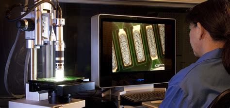
Automated Optical Inspection (AOI)
AOI uses high-resolution cameras and advanced image processing algorithms to automatically detect defects on the PCB surface. This method is faster and more accurate than visual inspection, making it ideal for high-volume production. AOI can identify issues such as:
- Solder bridging or insufficient solder
- Component misalignment or absence
- Incorrect component polarity
- Damaged or lifted pads
X-Ray Inspection
X-ray inspection is used to examine the internal structure of the PCB, particularly for hidden defects that cannot be detected by visual or AOI methods. This technique is especially useful for inspecting:
- Ball Grid Array (BGA) and other surface-mount devices with hidden solder joints
- Voids or cracks in solder joints
- Incorrect component placement or orientation
In-Circuit Testing (ICT)
ICT involves using a specialized fixture to make electrical contact with the PCB and test the functionality of individual components and circuits. This method can detect:
- Short circuits or open connections
- Incorrect component values or tolerances
- Defective or missing components

PCB Inspection Checklist
To ensure a thorough and systematic approach to PCB inspection, it is essential to follow a comprehensive checklist. A typical PCB inspection checklist may include the following items:
- Board Cosmetic Inspection
- Check for any visible damage, scratches, or discoloration on the PCB surface
-
Verify the presence and legibility of markings, labels, and designators
-
Component Placement Inspection
- Ensure all components are present and correctly placed according to the assembly drawing
- Check Component orientation and polarity
-
Verify component values and tolerances
-
Solder Joint Inspection
- Examine solder joints for proper wetting, fillets, and shape
- Check for solder bridging, insufficiency, or excess
-
Inspect for any lifted pads or damaged traces
-
Clearance and Spacing Inspection
- Verify that components and traces maintain the required clearance and spacing
-
Check for any potential short circuits or interference between components
-
Cleanliness Inspection
- Ensure the PCB is free from flux residue, dirt, or other contaminants
-
Check for any foreign objects or debris on the board surface
-
Functional Testing
- Perform in-circuit testing to verify the functionality of individual components and circuits
- Conduct system-level testing to ensure the overall performance and reliability of the assembled PCB

Best Practices for Effective PCB Inspection
To optimize the efficiency and accuracy of PCB inspection, consider implementing the following best practices:
-
Establish clear quality standards and acceptance criteria based on industry guidelines and customer requirements.
-
Invest in advanced inspection equipment and software to automate and streamline the inspection process.
-
Provide regular training and certification for inspection personnel to ensure they have the necessary skills and knowledge.
-
Implement a robust documentation and reporting system to track inspection results, defects, and corrective actions.
-
Continuously monitor and analyze inspection data to identify trends, root causes, and opportunities for process improvement.

Common PCB Defects and Their Causes
| Defect Type | Possible Causes |
|---|---|
| Solder Bridging | – Excessive solder paste – Improper solder stencil design – Incorrect reflow profile |
| Component Misalignment | – Incorrect pick-and-place programming – Damaged or worn placement nozzles – Inadequate component securement |
| Lifted Pads | – Excessive thermal stress during reflow – Poor PCB design or material selection – Improper handling or storage |
| Solder Voids | – Insufficient solder paste volume – Inadequate flux activation – Incorrect reflow profile or cooling rate |
| Tombstoning | – Uneven solder paste distribution – Mismatched component and pad sizes – Rapid heating or cooling during reflow |
By understanding the common defects and their underlying causes, manufacturers can take proactive measures to prevent their occurrence and improve the overall quality of PCB assembly.
Frequently Asked Questions (FAQ)
- What is the difference between AOI and X-ray inspection?
-
AOI uses high-resolution cameras to inspect the surface of the PCB, while X-ray inspection examines the internal structure of the board, including hidden solder joints and components.
-
How often should PCB inspection be performed during the assembly process?
-
PCB inspection should be conducted at various stages of the assembly process, including after solder paste printing, component placement, and reflow soldering. A final inspection should also be performed before packaging and shipping.
-
Can PCB inspection guarantee 100% defect-free products?
-
While PCB inspection can significantly reduce the occurrence of defects, it is not possible to guarantee 100% defect-free products due to the inherent limitations of inspection techniques and human error. However, implementing a comprehensive inspection process can help minimize the risk of defects and ensure high product quality.
-
What are the benefits of using automated inspection systems for PCB assembly?
-
Automated inspection systems, such as AOI and X-ray machines, offer several benefits, including faster inspection speeds, higher accuracy, and better repeatability compared to manual inspection methods. They also enable the collection and analysis of inspection data for continuous process improvement.
-
How can manufacturers balance the cost and effectiveness of PCB inspection?
- Manufacturers can optimize the cost and effectiveness of PCB inspection by adopting a risk-based approach, focusing on critical components and high-risk areas of the board. They can also invest in advanced inspection technologies that provide the best return on investment in terms of defect detection and process efficiency.
Conclusion
The final inspection of PCB assembly is a critical step in ensuring the quality, reliability, and performance of electronic devices. By employing a combination of visual, automated, and functional inspection techniques, manufacturers can identify and address potential defects before the products reach the end-users. Implementing best practices, such as establishing clear quality standards, investing in advanced inspection equipment, and providing regular training for personnel, can further enhance the effectiveness of the inspection process. As the electronics industry continues to evolve, with increasing complexity and miniaturization of components, the importance of robust PCB inspection will only grow in the future.


Leave a Reply