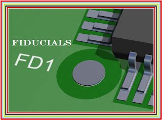
What are PCB Fiducials?
PCB fiducials, also known as fiducial markers or alignment marks, are small copper circles or other shapes etched onto printed circuit boards (PCBs) that serve as reference points for assembling, inspecting, and testing the boards. Fiducials help machines precisely locate and orient the PCB during automated assembly processes like solder paste application, component placement, and optical inspection.
Fiducial markers are critical for ensuring the accuracy and consistency of PCB Assembly, especially for high-density boards with small components. By providing a common reference system for machines and vision systems, fiducials enable the precise alignment of the PCB, stencil, and pick-and-place equipment, minimizing errors and improving production yields.
Types of PCB Fiducials
There are two main types of fiducials used in PCB manufacturing:
-
Global Fiducials: Also called panel fiducials or board fiducials, these markers are placed on the edges or corners of the PCB panel and provide a reference for the entire board. Global fiducials are used to align the PCB with the stencil during solder paste application and to locate the board in the pick-and-place machine.
-
Local Fiducials: Also known as component fiducials, these markers are placed near specific components or groups of components on the PCB. Local fiducials provide a more precise reference for placing individual components, especially those with fine pitch leads or small footprints. They are particularly useful for high-density boards or when using advanced packaging technologies like chip-scale packages (CSPs) or ball grid arrays (BGAs).
Here’s a table comparing global and local fiducials:
| Feature | Global Fiducials | Local Fiducials |
|---|---|---|
| Location | Edges or corners of PCB panel | Near specific components |
| Function | Align PCB with stencil and pick-and-place | Precisely place individual components |
| Quantity | Typically 3 or more per panel | Varies based on component density |
| Size | Larger (1-3 mm diameter) | Smaller (0.5-1 mm diameter) |
| Importance | Critical for overall board alignment | Important for high-density or fine-pitch components |

Fiducial Design Guidelines
To ensure that fiducials are easily recognizable by vision systems and provide accurate reference points, follow these design guidelines:
-
Shape: Use circular fiducials whenever possible, as they provide the most consistent reference point regardless of viewing angle. If necessary, other simple geometric shapes like squares or diamonds can be used.
-
Size: For global fiducials, use a diameter of 1-3 mm. Local fiducials should be smaller, typically 0.5-1 mm in diameter, to avoid interfering with nearby components.
-
Clearance: Provide sufficient clearance around fiducials to ensure they are easily distinguishable from surrounding features. A minimum clearance of 3-5 times the fiducial diameter is recommended.
-
Copper Weight: Use the same copper weight for fiducials as for other PCB features to ensure consistent etching and avoid discrepancies in the final marker size.
-
Solder Mask: Fiducials should be free of solder mask to provide the best contrast for vision systems. Define solder mask clearance in your CAD software to ensure the markers are fully exposed.
-
Location: Place global fiducials near the corners of the PCB panel, preferably outside the board outline to avoid interfering with the final product. Local fiducials should be placed as close as possible to the components they reference without overlapping or interfering with pads or traces.
Here are some common fiducial sizes and their applications:
| Fiducial Size (mm) | Application |
|---|---|
| 1.0 | Small PCBs, local fiducials |
| 1.5 | Medium-sized PCBs, local fiducials |
| 2.0 | Large PCBs, global fiducials |
| 2.5 | Very large PCBs, global fiducials |
| 3.0 | Oversized global fiducials for special applications |

Placing Fiducials on Your PCB
When designing your PCB, consider the following factors for placing fiducials:
-
Quantity: Use a minimum of three global fiducials per PCB panel, preferably near the corners. This allows the vision system to accurately determine the board’s position and orientation. For local fiducials, use as many as necessary to ensure precise component placement, especially for high-density areas.
-
Symmetry: Place global fiducials symmetrically around the PCB panel to minimize the impact of any dimensional variations or distortions. This helps ensure consistent alignment across the entire board.
-
Interference: Avoid placing fiducials too close to other PCB features like pads, traces, or vias. This can make it difficult for vision systems to distinguish the markers and may lead to placement errors.
-
Accessibility: Ensure that fiducials are easily accessible for vision systems and not obstructed by tall components or other features on the assembled board.
Here’s an example of global fiducial placement on a PCB panel:
+---------------------------+
|                           |
|     +---+           +---+ |
|     |   |           |   | |
|     +---+           +---+ |
|                           |
|                           |
|     +---+                 |
|     |   |                 |
|     +---+                 |
|                           |
+---------------------------+
In this diagram, the three global fiducials are placed near the corners of the panel, providing a stable reference for the entire board.

Verifying Fiducial Placement
After designing your PCB and placing fiducials, it’s essential to verify their placement and ensure they meet the requirements of your manufacturing process. Here are some steps to follow:
-
Review Design Rules: Check your CAD software’s design rule settings to ensure that fiducials meet the specified size, shape, and clearance requirements.
-
Generate Gerber Files: Export your PCB design as Gerber files, which are the industry standard for PCB fabrication. Make sure to include the necessary layers, such as copper, solder mask, and silkscreen.
-
Inspect Gerber Files: Use a Gerber viewer to inspect the exported files and verify that fiducials are correctly placed and sized. Check for any discrepancies or errors that may have occurred during the export process.
-
Communicate with Manufacturer: Provide your PCB manufacturer with the Gerber files and any additional instructions or requirements related to fiducials. Discuss any concerns or questions they may have to ensure a smooth manufacturing process.
By following these steps, you can help ensure that your PCB fiducials are correctly placed and will provide accurate reference points for assembly and inspection.
FAQ
-
Q: What is the minimum number of global fiducials required for a PCB?
A: A minimum of three global fiducials is recommended for a PCB panel to ensure accurate alignment and orientation. -
Q: Can I use non-circular shapes for fiducials?
A: While circular fiducials are preferred, other simple geometric shapes like squares or diamonds can be used if necessary. -
Q: How do I ensure fiducials are not covered by solder mask?
A: In your CAD software, define a solder mask clearance around the fiducials to ensure they remain exposed after the solder mask is applied. -
Q: What should I do if my PCB manufacturer has specific requirements for fiducials?
A: Always communicate with your PCB manufacturer and follow their guidelines for fiducial placement and design. They may have specific requirements based on their equipment and processes. -
Q: Can I use the same fiducials for solder paste application and component placement?
A: Yes, the same global fiducials can be used for both solder paste application and component placement, as long as they meet the size and clearance requirements for both processes.
Conclusion
PCB fiducials play a crucial role in ensuring the accuracy and consistency of automated PCB assembly processes. By understanding the types of fiducials, their design guidelines, and placement considerations, you can create PCBs that are optimized for manufacturing and help minimize errors and improve production yields.
When designing your PCB, remember to:
- Use a minimum of three global fiducials per panel, placed symmetrically near the corners
- Follow the recommended size and clearance guidelines for both global and local fiducials
- Verify fiducial placement in your CAD software and Gerber files
- Communicate with your PCB manufacturer to ensure compatibility with their processes
By following these best practices, you can streamline your PCB manufacturing process, reduce costs, and improve the overall quality of your products.


Leave a Reply