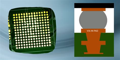
How Via-in-pad plating Works
In a conventional PCB design, vias are typically located outside the surface mount pads to avoid interfering with the soldering process. However, as electronic devices become more compact and complex, there is an increasing demand for higher-density PCB layouts. Via-in-pad plating addresses this challenge by placing the vias directly under the surface mount pads, allowing for more efficient use of board space.
The via-in-pad plating process involves the following steps:
-
Drilling: Holes are drilled through the PCB substrate at the desired via locations, including those under the surface mount pads.
-
Plating: The drilled holes are then plated with a conductive material, typically copper, to create the vias. The plating process also covers the surface mount pads, creating a continuous conductive surface.
-
Filling: After plating, the vias are filled with a non-conductive material, such as epoxy or resin, to provide a flat surface for component placement and to prevent solder from wicking down the via during the soldering process.
-
Solder mask application: A solder mask is applied over the PCB surface, leaving the surface mount pads and the filled vias exposed.
-
Surface finish: A surface finish, such as ENIG (Electroless Nickel Immersion Gold) or HASL (Hot Air Solder Leveling), is applied to the exposed pads and vias to protect the copper from oxidation and to enhance solderability.
Benefits of Via-in-Pad Plating
Via-in-pad plating offers several advantages over traditional PCB layouts:
1. Increased Component Density
By placing vias directly under the surface mount pads, via-in-pad plating allows for a more compact PCB layout. This increased component density is particularly beneficial for small form factor devices, such as smartphones, wearables, and IoT sensors, where board space is at a premium.
2. Improved Signal Integrity
Via-in-pad plating can improve signal integrity by reducing the distance between the component and the via, minimizing the inductance and resistance associated with longer trace lengths. This is especially important for high-speed digital circuits, where signal integrity is critical for proper operation.
3. Enhanced Thermal Performance
Vias placed under the surface mount pads can act as thermal vias, providing a direct path for heat dissipation from the component to the PCB substrate. This enhanced thermal performance can help to improve the reliability and longevity of electronic devices, particularly those with high-power components.
4. Better Mechanical Stability
Via-in-pad plating can improve the mechanical stability of surface-mounted components by providing a more secure connection between the component and the PCB. The filled vias act as anchors, reducing the risk of component damage due to mechanical stress or vibration.

Challenges and Considerations
While via-in-pad plating offers numerous benefits, there are also some challenges and considerations to keep in mind when designing and manufacturing PCBs with this technology:
1. Manufacturing Complexity
Via-in-pad plating requires more advanced manufacturing processes compared to traditional PCB layouts. The drilling, plating, and filling steps must be carefully controlled to ensure the vias are properly formed and filled, and the surface mount pads are not damaged during the process.
2. Cost
The additional manufacturing steps involved in via-in-pad plating can increase the cost of PCB fabrication compared to standard designs. However, the cost increase may be offset by the benefits of higher component density, improved performance, and reduced overall device size.
3. Design Constraints
Via-in-pad plating may impose certain design constraints, such as minimum pad size and via diameter, to ensure proper manufacturing and assembly. PCB designers must carefully consider these constraints when creating layouts and work closely with the fabrication and assembly partners to ensure compatibility.
4. Assembly Challenges
The presence of filled vias under the surface mount pads can create challenges during the assembly process, particularly with regard to solder paste printing and component placement. Specialized equipment and processes may be required to ensure accurate and reliable assembly of via-in-pad PCBs.

Applications of Via-in-Pad Plating
Via-in-pad plating is particularly well-suited for applications that require high component density, improved signal integrity, and enhanced thermal performance. Some common applications include:
1. Mobile Devices
Smartphones, tablets, and wearables often employ via-in-pad plating to maximize board space utilization and enable the integration of advanced features and functionalities within a compact form factor.
2. High-Speed Digital Devices
Devices that rely on high-speed digital interfaces, such as USB, HDMI, and PCI Express, can benefit from the improved signal integrity provided by via-in-pad plating. The reduced inductance and resistance associated with shorter trace lengths can help to minimize signal distortion and ensure reliable data transmission.
3. Automotive Electronics
The harsh operating environment and stringent reliability requirements of automotive electronics make via-in-pad plating an attractive option for these applications. The enhanced mechanical stability and thermal performance offered by via-in-pad plating can help to ensure the long-term reliability of automotive electronic systems.
4. Internet of Things (IoT) Devices
IoT devices, such as sensors, actuators, and communication modules, often require compact, high-density PCB layouts to fit within small form factors. Via-in-pad plating enables the integration of more functionality within a limited board space, making it an ideal choice for many IoT applications.

FAQ
1. What is the difference between via-in-pad plating and traditional PCB layouts?
In traditional PCB layouts, vias are typically placed outside the surface mount pads to avoid interfering with the soldering process. Via-in-pad plating, on the other hand, involves placing the vias directly under the surface mount pads, allowing for more efficient use of board space and improved signal integrity.
2. What are the main benefits of via-in-pad plating?
The main benefits of via-in-pad plating include increased component density, improved signal integrity, enhanced thermal performance, and better mechanical stability compared to traditional PCB layouts.
3. What are some challenges associated with via-in-pad plating?
Some challenges associated with via-in-pad plating include increased manufacturing complexity, higher fabrication costs, design constraints, and potential assembly challenges related to solder paste printing and component placement.
4. What applications are best suited for via-in-pad plating?
Via-in-pad plating is particularly well-suited for applications that require high component density, improved signal integrity, and enhanced thermal performance, such as mobile devices, high-speed digital devices, automotive electronics, and IoT devices.
5. How does via-in-pad plating improve signal integrity?
Via-in-pad plating can improve signal integrity by reducing the distance between the component and the via, minimizing the inductance and resistance associated with longer trace lengths. This is especially important for high-speed digital circuits, where signal integrity is critical for proper operation.
Conclusion
Via-in-pad plating is an advanced PCB manufacturing process that offers numerous benefits over traditional PCB layouts, including increased component density, improved signal integrity, enhanced thermal performance, and better mechanical stability. By placing vias directly under the surface mount pads, via-in-pad plating enables the creation of more compact, high-performance electronic devices that can meet the demands of today’s increasingly complex and interconnected world.
While via-in-pad plating does present some challenges in terms of manufacturing complexity, cost, and design constraints, the benefits often outweigh these drawbacks, particularly for applications that require the highest levels of performance and reliability. As electronic devices continue to evolve and push the boundaries of what is possible, via-in-pad plating will likely play an increasingly important role in enabling the next generation of innovative products and solutions.


Leave a Reply