Introduction to Printed Circuit Boards (PCBs)
Printed Circuit Boards, commonly known as PCBs, are the backbone of modern electronic devices. They are used in a wide range of applications, from simple consumer electronics to complex industrial equipment and aerospace systems. PCBs provide a platform for electronic components to be mounted and interconnected, allowing for the creation of complex circuits in a compact and efficient manner.
Types of PCBs
There are several types of PCBs, each designed to meet specific requirements and applications. Some of the most common types include:
- Single-sided PCBs: These have conductive tracks on only one side of the board.
- Double-sided PCBs: These have conductive tracks on both sides of the board, allowing for more complex circuits and higher component density.
- Multi-layer PCBs: These consist of multiple layers of conductive tracks, separated by insulating layers, enabling even more complex circuits and higher component density.
- Flexible PCBs: These are made from flexible materials, allowing them to be bent or folded to fit into tight spaces or conform to specific shapes.
- Rigid-Flex PCBs: These combine the benefits of both rigid and flexible PCBs, with rigid sections for mounting components and flexible sections for connecting them.
Bare PCBs
What is a Bare PCB?
A bare PCB, also known as an unpopulated PCB, is a printed circuit board that has been manufactured but does not have any electronic components mounted on it. It consists of the substrate material, typically FR-4, with conductive tracks etched onto the surface to create the desired circuit pattern.
Manufacturing Process of Bare PCBs
The manufacturing process of bare PCBs involves several steps:
- Design: The circuit is designed using specialized software, such as Eagle or KiCad.
- Material Selection: The appropriate substrate material is chosen based on the application and requirements.
- Copper Cladding: A thin layer of copper is bonded to the substrate.
- Etching: The desired circuit pattern is etched onto the copper layer using a photoresist and chemical etching process.
- Drilling: Holes are drilled through the board to accommodate through-hole components and vias.
- Plating: The holes are plated with copper to create electrical connections between layers.
- Solder Mask Application: A protective layer, known as the solder mask, is applied to the board to insulate the copper traces and prevent short circuits.
- Silkscreen Printing: Text and symbols are printed onto the board for component identification and assembly guidance.
Applications of Bare PCBs
Bare PCBs are used in various scenarios, such as:
- Prototyping: Bare PCBs are often used for prototyping and testing new designs before mass production.
- Custom Projects: Hobbyists and engineers may use bare PCBs to create custom electronic projects.
- Education: Bare PCBs are used in educational settings to teach students about electronic circuits and PCB design.
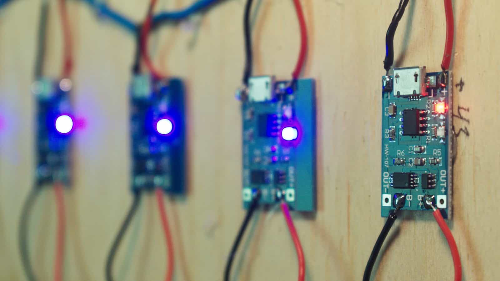
Populated PCBs
What is a Populated PCB?
A populated PCB, also known as an assembled PCB, is a printed circuit board that has electronic components mounted onto it. These components can include resistors, capacitors, integrated circuits (ICs), connectors, and various other electronic devices. The components are soldered onto the board, either through surface mount technology (SMT) or through-hole mounting.
Assembly Process of Populated PCBs
The assembly process of populated PCBs involves several steps:
- Solder Paste Application: A thin layer of solder paste is applied to the pads on the PCB where the components will be mounted.
- Component Placement: The electronic components are placed onto the PCB, either manually or using automated pick-and-place machines.
- Reflow Soldering: The PCB is heated in a reflow oven, causing the solder paste to melt and form electrical and mechanical connections between the components and the board.
- Inspection: The assembled PCB is inspected for any defects or mistakes, such as misaligned components or short circuits.
- Testing: The populated PCB is tested to ensure proper functionality and performance.
Applications of Populated PCBs
Populated PCBs are used in virtually every electronic device, including:
- Consumer Electronics: Smartphones, laptops, televisions, and home appliances all contain populated PCBs.
- Industrial Equipment: Machinery, control systems, and automation devices rely on populated PCBs for their operation.
- Medical Devices: Populated PCBs are used in various medical devices, such as pacemakers, imaging equipment, and diagnostic tools.
- Aerospace and Defense: Populated PCBs are critical components in aircraft, satellites, and military equipment.

Differences Between Bare PCBs and Populated PCBs
While bare PCBs and populated PCBs are both essential in the world of electronics, they have several key differences:
| Aspect | Bare PCBs | Populated PCBs |
|---|---|---|
| Components | No components mounted | Electronic components soldered onto the board |
| Functionality | Not functional on their own | Fully functional electronic assembly |
| Manufacturing Process | Involves designing, etching, drilling, and plating | Includes component placement and soldering in addition to bare PCB manufacturing |
| Cost | Less expensive than populated PCBs | More expensive due to additional components and assembly process |
| Applications | Prototyping, custom projects, education | Used in all electronic devices across various industries |
Frequently Asked Questions (FAQ)
1. Can I design my own PCB?
Yes, you can design your own PCB using specialized software such as Eagle, KiCad, or Altium Designer. These tools allow you to create schematic diagrams and layout the PCB design according to your requirements.
2. How long does it take to manufacture a bare PCB?
The manufacturing time for a bare PCB depends on various factors, such as the complexity of the design, the chosen material, and the manufacturer’s capacity. Typically, it can take anywhere from a few days to a couple of weeks to manufacture a bare PCB.
3. What is the difference between surface mount and through-hole components?
Surface mount components are mounted directly onto the surface of the PCB, while through-hole components have leads that are inserted into holes drilled through the board. Surface mount technology allows for smaller components and higher component density, while through-hole mounting provides stronger mechanical connections and is easier for manual assembly.
4. How do I choose the right substrate material for my PCB?
The choice of substrate material depends on the specific requirements of your application, such as the operating temperature, frequency, and environmental conditions. FR-4 is the most common substrate material for general-purpose PCBs, while other materials like polyimide or ceramics may be used for high-temperature or high-frequency applications.
5. Can populated PCBs be repaired if a component fails?
Yes, populated PCBs can be repaired by skilled technicians. The faulty component can be desoldered and replaced with a new one. However, the repair process can be challenging, especially for surface mount components and multi-layer boards, and may not always be economically feasible.
Conclusion
Understanding the difference between bare PCBs and populated PCBs is essential for anyone involved in the design, manufacturing, or use of electronic devices. Bare PCBs provide the foundation for electronic circuits, while populated PCBs bring those circuits to life with the addition of electronic components.
The manufacturing process for bare PCBs involves designing, etching, drilling, and plating, while populated PCBs require additional steps such as component placement and soldering. Bare PCBs are used for prototyping, custom projects, and education, while populated PCBs are found in virtually every electronic device across various industries.
As technology continues to advance, the demand for more complex and compact electronic devices will drive innovation in PCB design and manufacturing. By understanding the fundamentals of bare and populated PCBs, engineers and technicians can create more efficient, reliable, and innovative electronic solutions.


Leave a Reply