Understanding SMT Tombstoning
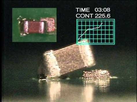
SMT (Surface Mount Technology) tombstoning is a common defect that occurs during the reflow soldering process in PCB (Printed Circuit Board) assembly. It is characterized by one end of a surface mount component, such as a chip resistor or capacitor, lifting off the PCB pad while the other end remains soldered. This phenomenon results in the component standing upright on the board, resembling a tombstone, hence the name “tombstoning.”
Causes of SMT Tombstoning
Several factors can contribute to the occurrence of SMT tombstoning:
-
Uneven heating: If one end of the component heats up faster than the other during the reflow process, it can cause the solder to melt and surface tension to pull the component upright.
-
Component size and shape: Smaller and lighter components, such as chip resistors and capacitors, are more prone to tombstoning due to their low mass and high surface area to volume ratio.
-
Pad design: Unequal pad sizes or improper pad spacing can lead to uneven solder joint formation, increasing the risk of tombstoning.
-
Solder paste application: Inconsistent or excessive solder paste deposition can cause an imbalance in the solder volume on the pads, leading to tombstoning.
-
Reflow profile: An improper reflow temperature profile, with rapid heating or cooling rates, can exacerbate the tombstoning effect.
Impact of SMT Tombstoning
SMT tombstoning can have several negative consequences on the PCB assembly process and the final product:
-
Reliability issues: Tombstoned components have poor or no electrical connection, leading to open circuits or intermittent failures in the assembled PCB.
-
Rework and repair: Tombstoned components require manual rework or replacement, increasing production time and costs.
-
Yield loss: High tombstoning rates can significantly reduce the overall production yield, affecting manufacturing efficiency and profitability.
-
Visual defects: Tombstoned components are easily noticeable and can affect the aesthetic appeal of the PCB, especially in consumer electronic products.

Preventing SMT Tombstoning
To minimize the occurrence of SMT tombstoning, several preventive measures can be implemented:
PCB Design Considerations
-
Pad design: Ensure that the component pads are of equal size and shape, with proper spacing between them. Follow the recommended land pattern dimensions provided by the component manufacturer.
-
Copper balance: Maintain a consistent copper balance on both sides of the component to promote even heating during reflow.
-
Solder mask design: Use solder mask between closely spaced pads to prevent solder bridging and maintain consistent solder joint formation.
Solder Paste Application
-
Stencil design: Optimize the stencil aperture size and shape to achieve consistent solder paste deposition on the pads.
-
Solder paste quality: Use high-quality solder paste with the appropriate particle size and flux chemistry for the specific application.
-
Printing process: Ensure proper printer setup, including squeegee pressure, speed, and separation distance, to achieve uniform solder paste deposition.
Reflow Profile Optimization
-
Temperature profile: Develop a reflow profile with a gradual ramp-up rate and a sufficient soaking zone to allow even heating of the components and PCB.
-
Peak temperature: Control the peak reflow temperature to minimize the temperature difference between the component and the PCB.
-
Cooling rate: Implement a controlled cooling rate to prevent rapid solidification of the solder joints, which can contribute to tombstoning.
Component Selection and Placement
-
Component size: Choose components with appropriate size and mass to reduce the risk of tombstoning. Larger components are generally less prone to tombstoning.
-
Placement accuracy: Ensure accurate component placement on the pads using a pick-and-place machine with high precision and repeatability.
-
Component orientation: Orient components in a way that minimizes the difference in thermal mass between the leads, reducing the likelihood of uneven heating.

Tombstone Detection and Rework
Despite preventive measures, tombstoning can still occur in SMT assembly. Effective detection and rework strategies are essential to maintain product quality and minimize yield loss.
Visual Inspection
-
Manual inspection: Trained operators can visually inspect the assembled PCBs for tombstoned components using magnification tools or microscopes.
-
Automated optical inspection (AOI): AOI systems can detect tombstoned components using advanced image processing algorithms and compare them against predefined templates.
X-Ray Inspection
-
2D X-ray: Two-dimensional X-ray inspection can reveal tombstoned components that may not be visible from the surface, especially for components with hidden leads or in densely populated areas.
-
3D X-ray: Three-dimensional X-ray inspection provides a more detailed view of the solder joints, enabling the detection of partially tombstoned components or other related defects.
Rework Process
-
Component removal: Tombstoned components are carefully removed using a soldering iron or a hot air rework station, ensuring minimal damage to the PCB pads and surrounding components.
-
Site preparation: The PCB pads are cleaned and prepared for the new component placement, removing any residual solder or contaminants.
-
Component replacement: A new component is placed on the pads using a pick-and-place machine or manual placement, ensuring proper alignment and orientation.
-
Reflow soldering: The reworked area is subjected to a localized reflow process using a focused heat source, such as a hot air nozzle or a laser, to form new solder joints.

Case Studies and Research
Several studies and research papers have investigated the causes, prevention, and detection of SMT tombstoning. Here are a few notable examples:
-
“Investigation of Tombstone Effect in SMT Components” (Puttlitz, K. J., et al., 2004): This study investigated the factors contributing to tombstoning in chip resistors and capacitors, including component size, pad design, and reflow profile. The authors proposed design guidelines and process optimizations to minimize tombstoning.
-
“Tombstone Effect Reduction by Optimizing the Reflow Profile” (Zhang, H., et al., 2008): This research focused on the impact of reflow profile parameters, such as ramp rate, soak time, and peak temperature, on tombstoning. The authors developed an optimized reflow profile that significantly reduced tombstoning rates in chip resistors.
-
“Detection of Tombstone Defects in SMT Assembly Using 2D and 3D X-Ray Imaging” (Kim, J., et al., 2015): This study compared the effectiveness of 2D and 3D X-ray inspection techniques in detecting tombstoned components. The authors demonstrated that 3D X-ray provided higher detection accuracy and the ability to identify partially tombstoned components.
Frequently Asked Questions (FAQ)
-
What is the main cause of SMT tombstoning?
The main cause of SMT tombstoning is uneven heating of the component leads during the reflow soldering process, which results in one end of the component lifting off the PCB pad while the other end remains soldered. -
Which components are most prone to tombstoning?
Smaller and lighter components, such as chip resistors and capacitors, are more prone to tombstoning due to their low mass and high surface area to volume ratio. -
How can PCB design help prevent tombstoning?
PCB design can help prevent tombstoning by ensuring equal pad sizes and shapes, proper pad spacing, consistent copper balance, and appropriate solder mask design. -
What role does solder paste application play in preventing tombstoning?
Consistent and uniform solder paste application, achieved through optimized stencil design and printing process, is crucial in preventing tombstoning by maintaining an equal solder volume on the component pads. -
How is tombstoning detected in SMT assembly?
Tombstoning can be detected through visual inspection, automated optical inspection (AOI), and X-ray inspection techniques, including 2D and 3D X-ray imaging.
Conclusion
SMT tombstoning is a common defect in PCB assembly that can lead to reliability issues, increased rework, and yield loss. Understanding the causes and implementing preventive measures in PCB design, solder paste application, reflow profile optimization, and component selection and placement can significantly reduce the occurrence of tombstoning.
Effective detection methods, such as visual inspection, AOI, and X-ray inspection, are essential for identifying tombstoned components and facilitating timely rework. By adopting best practices and continuous process improvement, manufacturers can minimize the impact of SMT tombstoning and enhance the quality and reliability of their PCB assemblies.
As the electronics industry continues to evolve, with the increasing complexity and miniaturization of components, addressing SMT tombstoning will remain a critical aspect of PCB assembly. Ongoing research and development efforts in materials, processes, and inspection technologies will contribute to the advancement of tombstone prevention and detection strategies, enabling the production of high-quality and reliable electronic products.


Leave a Reply