Understanding Surface Mount Technology (SMT)
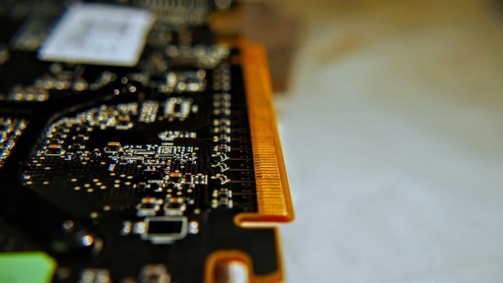
SMT is a modern PCB assembly technique that involves mounting electronic components directly onto the surface of a printed circuit board. Unlike through-hole technology, where component leads are inserted into drilled holes and soldered on the opposite side of the board, SMT components have small metal tabs or leads that are soldered directly onto the board’s surface.
Key Features of SMT
- Smaller component sizes
- Higher component density
- Automated assembly process
- Improved reliability and performance
- Reduced manufacturing costs
Advantages of SMT in PCB Manufacturing
SMT offers several significant advantages over traditional through-hole technology. These advantages have made SMT the preferred choice for PCB manufacturers worldwide.
1. Miniaturization and Space Savings
One of the primary advantages of SMT is the ability to use smaller components, which leads to significant space savings on the PCB. SMT components are typically 50% smaller than their through-hole counterparts, allowing for higher component density and more compact PCB designs. This miniaturization is crucial for modern electronic devices, such as smartphones, wearables, and IoT devices, where space is at a premium.
2. Improved Performance and Reliability
SMT components offer improved performance and reliability compared to through-hole components. The smaller lead lengths and direct mounting on the PCB surface reduce parasitic capacitance and inductance, resulting in better signal integrity and higher-frequency performance. Additionally, SMT components are less susceptible to mechanical stress and vibration, leading to enhanced reliability and longer product life.
3. Automated Assembly and Lower Manufacturing Costs
SMT enables a highly automated assembly process, which significantly reduces manufacturing costs and increases production efficiency. SMT assembly lines utilize pick-and-place machines, solder paste printers, and reflow ovens to accurately place and solder components onto the PCB. This automation minimizes human error, improves consistency, and allows for faster production rates. As a result, SMT is more cost-effective for high-volume production runs compared to through-hole technology.
4. Design Flexibility and Innovation
SMT provides designers with greater flexibility in PCB layout and component placement. The smaller component sizes and absence of drilled holes allow for more creative and efficient PCB designs. This flexibility enables designers to incorporate advanced features, such as multi-layer boards, high-density interconnects (HDI), and embedded components. SMT also facilitates the adoption of new component packages, such as ball grid arrays (BGAs) and quad flat no-leads (QFNs), which offer higher pin counts and improved thermal performance.
SMT Assembly Process
The SMT assembly process involves several key steps that ensure the accurate placement and soldering of components onto the PCB. Understanding these steps is essential for designing and manufacturing reliable SMT PCBs.
1. Solder Paste Printing
The first step in the SMT assembly process is solder paste printing. A stainless steel stencil with apertures corresponding to the component pads is placed over the PCB. Solder paste, a mixture of tiny solder particles and flux, is then applied onto the stencil and spread using a squeegee. The solder paste is deposited onto the component pads through the stencil apertures, creating a precise pattern for component placement.
2. Component Placement
After solder paste printing, the PCB moves to the pick-and-place machine for component placement. The pick-and-place machine uses a computer-controlled robotic arm equipped with a vacuum nozzle to pick up SMT components from tape reels or trays and place them onto the solder paste deposits on the PCB. The machine’s vision system ensures accurate component alignment and orientation. High-speed pick-and-place machines can place thousands of components per hour, making the process highly efficient.
3. Reflow Soldering
Once all the components are placed, the PCB undergoes reflow soldering. The board is passed through a reflow oven, which applies a precisely controlled temperature profile to melt the solder paste and form a permanent electrical and mechanical connection between the components and the PCB. The reflow process typically involves four stages: preheat, thermal soak, reflow, and cooling. The temperature profile is carefully optimized to ensure proper solder joint formation and to minimize thermal stress on the components.
4. Inspection and Testing
After reflow soldering, the PCB undergoes inspection and testing to ensure the quality and reliability of the solder joints and the overall assembly. Automated optical inspection (AOI) systems use high-resolution cameras and advanced image processing algorithms to detect defects such as bridging, insufficient solder, or misaligned components. In-circuit testing (ICT) and functional testing are also performed to verify the electrical performance and functionality of the assembled PCB.

SMT Component Packages
SMT has enabled the development of various component packages that are optimized for surface mounting. These packages offer different advantages in terms of size, pin count, thermal performance, and assembly efficiency. Some common SMT component packages include:
- Small Outline Integrated Circuit (SOIC)
- Quad Flat Package (QFP)
- Ball Grid Array (BGA)
- Quad Flat No-Lead (QFN)
- Chip Scale Package (CSP)
| Package | Description | Advantages |
|---|---|---|
| SOIC | Rectangular package with gull-wing leads on two sides | Compact size, easy to solder, suitable for low to medium pin count devices |
| QFP | Square or rectangular package with gull-wing leads on four sides | Higher pin count than SOIC, good thermal performance, suitable for complex ICs |
| BGA | Package with an array of solder balls on the bottom surface | High pin count, excellent thermal performance, compact size |
| QFN | Leadless package with exposed pad on the bottom surface | Very small size, good thermal performance, low inductance and resistance |
| CSP | Package with dimensions close to the die size | Extremely small size, high-density interconnects, ideal for space-constrained applications |
Applications of SMT in PCB Manufacturing
SMT has found widespread adoption across various industries and applications due to its numerous advantages. Some key applications of SMT in PCB manufacturing include:
- Consumer Electronics
- Smartphones, tablets, and laptops
- Wearable devices and smartwatches
-
Gaming consoles and entertainment systems
-
Automotive Electronics
- Engine control units (ECUs)
- Infotainment systems and displays
-
Advanced driver assistance systems (ADAS)
-
Medical Devices
- Implantable devices and wearable monitors
- Diagnostic equipment and imaging systems
-
Portable medical instruments
-
Industrial Automation and IoT
- Factory automation systems and sensors
- Smart home devices and appliances
-
Wireless communication modules and gateways
-
Aerospace and Defense
- Avionics and flight control systems
- Radar and communication equipment
- Satellite and spacecraft electronics
Frequently Asked Questions (FAQ)
-
Q: What is the difference between SMT and through-hole technology?
A: SMT involves mounting components directly onto the surface of the PCB, while through-hole technology requires components to be inserted into drilled holes and soldered on the opposite side of the board. SMT components are smaller, allow for higher density, and enable automated assembly, while through-hole components are larger and require manual soldering. -
Q: Can SMT and through-hole components be used together on the same PCB?
A: Yes, it is possible to use both SMT and through-hole components on the same PCB. This is known as a mixed-technology or hybrid assembly. However, the assembly process becomes more complex, as it requires both SMT and through-hole soldering techniques. -
Q: What are the challenges associated with SMT assembly?
A: Some challenges in SMT assembly include the need for precise solder paste printing, accurate component placement, and proper reflow soldering. Thermal management can also be a concern, especially for high-density PCBs with a large number of components. Additionally, the small size of SMT components can make manual rework and repair more difficult compared to through-hole components. -
Q: How does the choice of solder paste affect SMT assembly?
A: The selection of solder paste is crucial for successful SMT assembly. The solder paste must have the right viscosity, particle size, and flux chemistry to ensure proper solder joint formation. The solder paste also needs to be compatible with the reflow temperature profile and the component materials. Improper solder paste selection can lead to defects such as bridging, insufficient solder, or poor wetting. -
Q: What are the key considerations when designing PCBs for SMT assembly?
A: When designing PCBs for SMT assembly, designers should consider factors such as component footprints, pad sizes, and spacing. Proper placement of components is essential to ensure accessibility for automated pick-and-place machines. Designers should also consider the reflow temperature profile and thermal management requirements. Additionally, designing for manufacturability (DFM) guidelines should be followed to minimize assembly defects and improve yield.
Conclusion
Surface Mount Technology (SMT) has transformed the PCB manufacturing industry, enabling the production of smaller, faster, and more reliable electronic devices. By allowing for miniaturization, improved performance, automated assembly, and cost-effective manufacturing, SMT has become the dominant technology in PCB assembly.
As electronic devices continue to evolve and demand for high-density, high-performance PCBs grows, SMT will remain at the forefront of PCB manufacturing. Designers and manufacturers must stay updated with the latest advancements in SMT components, assembly processes, and design techniques to ensure the successful development and production of cutting-edge electronic products.
By understanding the principles, advantages, and applications of SMT in PCB manufacturing, engineers, and technicians can leverage this powerful technology to create innovative and reliable electronic solutions for a wide range of industries and applications.


Leave a Reply