Types of PCB Projects
PCB projects can be categorized based on their complexity, application, and the skills required to complete them. Some common types of PCB projects include:
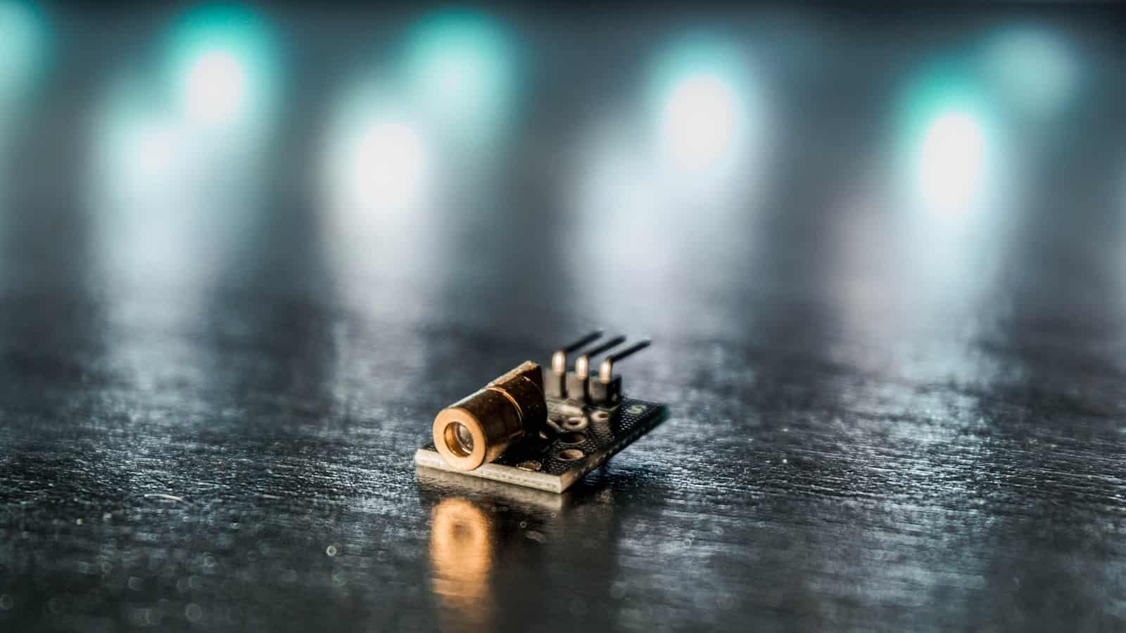
Hobby Projects
Hobby PCB projects are typically small-scale, simple designs that are undertaken for personal enjoyment, learning, or experimentation. These projects often involve creating custom PCBs for DIY electronic devices, such as:
- Arduino-based projects
- LED lighting projects
- Simple sensor circuits
- Audio amplifiers
- Radio transmitters and receivers
Educational Projects
Educational PCB projects are designed to help students learn about electronic circuit design, PCB layout, and assembly. These projects are often part of a curriculum in electronics engineering courses or workshops. Examples of educational PCB projects include:
- Basic logic circuits
- Temperature and light sensors
- Motor control circuits
- Simple power supplies
- Microcontroller-based projects
Professional Projects
Professional PCB projects are more complex and are typically undertaken by experienced engineers or technicians for commercial or industrial applications. These projects often involve designing PCBs for:
- Consumer electronics
- Medical devices
- Automotive electronics
- Industrial control systems
- Telecommunications equipment
PCB Design Process
The PCB design process involves several steps, from conceptualization to final assembly. The main stages of a PCB project include:
-
Schematic Design: The first step is to create a schematic diagram of the electronic circuit, which shows the components and their interconnections. This can be done using electronic design automation (EDA) software, such as KiCad, Eagle, or Altium Designer.
-
Component Selection: Once the schematic is complete, the next step is to select the appropriate components for the project. This involves choosing components based on their electrical specifications, package size, and cost.
-
PCB Layout: After the components are selected, the PCB layout is created using EDA software. The layout involves arranging the components on the board and routing the traces to connect them according to the schematic. The layout must also consider factors such as signal integrity, power distribution, and manufacturability.
-
PCB Fabrication: Once the layout is finalized, the PCB design files are sent to a PCB manufacturer for fabrication. The manufacturer will produce the physical PCB based on the provided design files.
-
PCB Assembly: After the PCB is fabricated, the components are soldered onto the board. This can be done manually for small-scale projects or using automated assembly processes for larger production runs.
-
Testing and Debugging: The final step is to test the assembled PCB to ensure it functions as intended. If any issues are found, debugging is performed to identify and resolve the problems.
Tools and Resources for PCB Projects
There are many tools and resources available for those interested in PCB projects, ranging from software to hardware and online communities.
EDA Software
Electronic Design Automation (EDA) software is essential for designing PCBs. Some popular EDA tools include:
| Software | Description | Pricing |
|---|---|---|
| KiCad | Open-source, cross-platform EDA suite for schematic and PCB design | Free |
| Eagle | Widely-used EDA software with a large component library | Subscription-based |
| Altium Designer | Professional-grade EDA software with advanced features | Paid |
| Autodesk Fusion 360 | CAD software with electronics design capabilities | Subscription-based |
PCB Fabrication and Assembly Services
Once the PCB design is complete, it needs to be fabricated and assembled. There are many online services that offer PCB fabrication and assembly, such as:
| Service | Description | Pricing |
|---|---|---|
| JLCPCB | Low-cost PCB fabrication and assembly services | Varies based on specifications |
| PCBWay | PCB fabrication, assembly, and 3D printing services | Varies based on specifications |
| OSH Park | Community-driven PCB fabrication service with a focus on open-source designs | Varies based on specifications |
| Seeed Studio | PCB fabrication, assembly, and component sourcing services | Varies based on specifications |
Online Communities and Resources
There are many online communities and resources dedicated to PCB design and electronics projects. Some popular ones include:
| Resource | Description |
|---|---|
| Hackaday | Online community for electronics enthusiasts, featuring project showcases, tutorials, and forums |
| Instructables | User-generated content platform with a wide range of electronics projects and tutorials |
| SparkFun Electronics | Online retailer of electronics components and tools, with a strong focus on education and community |
| Adafruit Industries | Online retailer of electronics components and tools, with a focus on open-source hardware and education |
| Arduino Forum | Official forum for the Arduino community, with discussions on projects, troubleshooting, and general electronics topics |

FAQ
-
What skills do I need to start a PCB project?
To start a PCB project, you should have a basic understanding of electronic circuits, components, and schematic symbols. Familiarity with EDA software and PCB layout principles is also helpful. If you are new to PCB design, many online tutorials and resources can help you get started. -
How much does it cost to fabricate a custom PCB?
The cost of PCB fabrication varies depending on factors such as the board size, number of layers, quantity, and turnaround time. Many online PCB fabrication services offer low-cost options for small-batch production, with prices starting at around $5 for a simple, single-layer board. -
What are the most common mistakes in PCB design?
Some common mistakes in PCB design include poor component placement, incorrect trace widths, lack of proper grounding, signal integrity issues, and failure to consider manufacturability. It is essential to follow best practices and guidelines for PCB design to avoid these mistakes. -
Can I design a PCB without using EDA software?
While it is possible to design a simple PCB by hand, using EDA software is highly recommended for most projects. EDA tools make the design process more efficient, accurate, and easier to iterate. They also provide features like design rule checks, which help catch errors before fabrication. -
How do I choose the right components for my PCB project?
When selecting components for your PCB project, consider factors such as the electrical specifications, package size, cost, and availability. It is essential to choose components that meet the requirements of your circuit and are compatible with your PCB layout. Datasheets and online component distributors can provide valuable information to help you make informed decisions.
In conclusion, PCB projects offer a wide range of opportunities for electronics enthusiasts, students, and professionals to create custom electronic devices and systems. By understanding the PCB design process, utilizing the available tools and resources, and following best practices, anyone can embark on their own PCB project journey. Whether you are a beginner looking to learn more about electronics or an experienced engineer working on a complex design, PCB projects provide a rewarding and engaging way to bring your ideas to life.


Leave a Reply