The Importance of PCB Microsections
PCB microsections play a crucial role in the electronics industry, as they help manufacturers and engineers to:
- Verify the quality of the PCB-Assembly.com/?p=2190″>PCB Manufacturing process
- Identify potential defects and failure points
- Ensure that the PCB meets the required specifications and standards
- Troubleshoot and analyze PCB failures
- Improve the overall reliability and performance of the PCB
Types of PCB Microsections
There are two main types of PCB microsections:
-
Cross-sectional microsections: These involve cutting the PCB perpendicular to the surface, allowing for the examination of the internal layers, plated through-holes, and vias.
-
Surface microsections: These involve cutting the PCB parallel to the surface, allowing for the examination of the surface features, such as traces, pads, and solder joints.
The PCB Microsectioning Process
The PCB microsectioning process typically involves the following steps:
-
Sample preparation: The PCB sample is cut to the desired size and location using a precision saw or laser cutter.
-
Mounting: The sample is then mounted in a suitable medium, such as epoxy resin, to provide support and stability during the grinding and polishing process.
-
Grinding and polishing: The mounted sample is ground and polished using progressively finer abrasive materials to create a smooth, flat surface suitable for microscopic examination.
-
Etching: In some cases, the polished surface may be etched using a chemical solution to reveal the internal structure of the PCB, such as the grain structure of the copper traces.
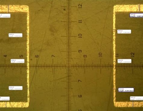
-
Microscopic examination: The prepared sample is then examined under a microscope, typically using a combination of bright-field and dark-field illumination techniques to highlight different features of the PCB.
Analyzing PCB Microsections
When analyzing PCB microsections, engineers and quality control specialists look for various features and potential defects, such as:
- Plating thickness and uniformity
- Proper registration and alignment of layers
- Void formation in plated through-holes and vias
- Delamination between layers
- Cracks or fractures in the PCB substrate or copper traces
- Solder joint quality and integrity
| Feature | Acceptable Range | Potential Issues |
|---|---|---|
| Plating thickness | 25-35 μm | Insufficient coverage, poor electrical performance |
| Layer registration | ±50 μm | Short circuits, open circuits |
| Void formation | <5% of hole area | Reduced mechanical strength, poor thermal dissipation |
| Delamination | None | Reduced mechanical strength, moisture ingress |
| Cracks or fractures | None | Electrical failures, mechanical weakness |
| Solder joint integrity | Complete coverage, no voids | Poor electrical and mechanical connections |
Advantages of PCB Microsections
PCB microsections offer several advantages over other PCB analysis techniques:
- They provide a detailed, high-resolution view of the internal structure of the PCB
- They allow for the identification of defects that may not be visible through other methods, such as X-ray inspection or electrical testing
- They can be used to analyze both functional and non-functional PCBs
- They provide a permanent record of the PCB structure that can be used for future reference and analysis
# FAQs
-
Q: How long does the PCB microsectioning process typically take?
A: The entire process, from sample preparation to microscopic examination, can take several hours to a few days, depending on the complexity of the PCB and the number of samples being analyzed. -
Q: What types of microscopes are used for PCB microsection analysis?
A: Optical microscopes are the most common type used for PCB microsection analysis, although scanning electron microscopes (SEMs) may be used for higher magnification and resolution. -
Q: Can PCB microsections be used to analyze flexible PCBs?
A: Yes, PCB microsections can be used to analyze both rigid and flexible PCBs, although the sample preparation process may differ slightly for flexible PCBs. -
Q: Are there any industry standards governing PCB microsection analysis?
A: Yes, there are several industry standards that provide guidelines for PCB microsection analysis, including IPC-A-600, IPC-6012, and IPC-TM-650. -
Q: How can PCB manufacturers use the information gained from microsection analysis to improve their processes?
A: By identifying potential defects and areas for improvement through microsection analysis, PCB manufacturers can optimize their manufacturing processes, select better materials, and implement more stringent quality control measures to enhance the overall quality and reliability of their products.
In conclusion, PCB microsections are a powerful tool for analyzing the internal structure and quality of printed circuit boards. By providing detailed, high-resolution images of the PCB cross-section, microsections enable engineers and quality control specialists to identify potential defects, verify manufacturing processes, and ensure that the PCB meets the required specifications. As the electronics industry continues to evolve and demand higher-performance, more reliable PCBs, the role of PCB microsections in ensuring product quality and integrity will only become more critical.


Leave a Reply