Introduction to PCB Copper Layers
Printed Circuit Boards (PCBs) are essential components in modern electronic devices. They provide a platform for mounting and connecting electronic components, enabling the creation of complex circuits. One of the critical elements of a PCB is the copper layer. PCB copper layers play a vital role in the functionality, reliability, and performance of electronic devices. In this article, we will delve into the world of PCB copper layers, exploring their types, functions, and the factors that influence their selection.
What are PCB Copper Layers?
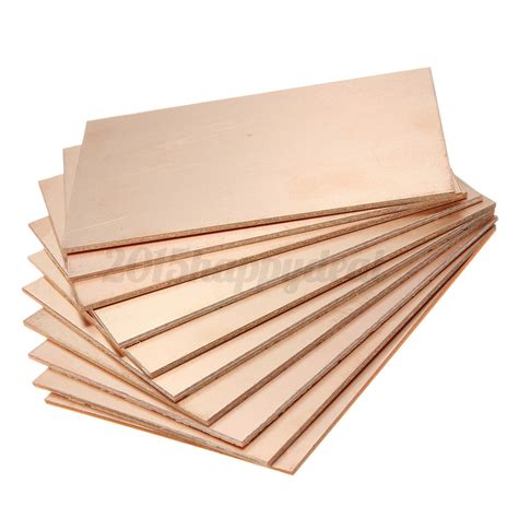
PCB copper layers are thin sheets of Copper Foil laminated onto a non-conductive substrate, typically made of fiberglass or epoxy resin. These layers form the conductive pathways that allow electrical signals to travel between components on the PCB. The copper layers are etched to create specific patterns, known as traces, which define the electrical connections between components.
Types of PCB Copper Layers
PCBs can have various numbers of copper layers, depending on the complexity and requirements of the circuit. The most common types of PCB copper layers are:
-
Single-layer PCB: A single-layer PCB has copper on only one side of the substrate. These PCBs are the simplest and most cost-effective option, suitable for basic circuits with low component density.
-
Double-layer PCB: Double-layer PCBs have copper on both sides of the substrate. They offer more routing options and higher component density compared to single-layer PCBs. Double-layer PCBs are widely used in consumer electronics and medium-complexity circuits.
-
Multi-layer PCB: Multi-layer PCBs have three or more layers of copper, separated by insulating layers. They provide the highest level of circuit complexity and density, allowing for the creation of intricate designs with numerous components. Multi-layer PCBs are commonly used in advanced electronic devices, such as smartphones, computers, and aerospace systems.

Functions of PCB Copper Layers
PCB copper layers serve several crucial functions in electronic circuits:
-
Signal Routing: The primary function of PCB copper layers is to route electrical signals between components. The etched traces on the copper layers form the conductive paths that allow signals to travel from one component to another, enabling the circuit to perform its intended function.
-
Power Distribution: PCB copper layers also play a vital role in distributing power to the components on the board. Dedicated power planes or wide traces are used to provide a low-impedance path for power distribution, ensuring stable and reliable power supply to the components.
-
Grounding: Proper grounding is essential for the stability and performance of electronic circuits. PCB copper layers are used to create ground planes, which provide a low-impedance return path for electrical currents. Ground planes help to reduce electromagnetic interference (EMI) and improve signal integrity.
-
Shielding: In some cases, PCB copper layers can be used for shielding sensitive circuits from external electromagnetic interference. By creating a Faraday cage around specific areas of the PCB, copper layers can help to isolate and protect sensitive components from unwanted signals.

Factors Influencing PCB Copper Layer Selection
When designing a PCB, several factors must be considered when selecting the appropriate number and configuration of copper layers:
-
Circuit Complexity: The complexity of the circuit is a primary factor in determining the number of copper layers required. Simple circuits with few components can often be implemented on single-layer or double-layer PCBs, while complex circuits with numerous components and intricate routing requirements may necessitate multi-layer PCBs.
-
Signal Integrity: Signal integrity refers to the quality and reliability of the electrical signals transmitted through the PCB. As the speed and frequency of signals increase, the likelihood of signal degradation and interference also increases. Multi-layer PCBs with dedicated signal layers and proper grounding techniques can help to maintain signal integrity in high-speed circuits.
-
Power Requirements: The power requirements of the circuit also influence the selection of PCB copper layers. Circuits with high current demands may require thicker copper layers or dedicated power planes to ensure adequate power distribution and minimize voltage drop.
-
Size Constraints: The available space for the PCB is another crucial factor in copper layer selection. In applications where PCB size is limited, such as in portable devices or IoT applications, multi-layer PCBs can provide a compact solution by allowing for higher component density and more efficient routing.
-
Cost Considerations: The number of copper layers directly impacts the manufacturing cost of the PCB. Single-layer and double-layer PCBs are generally less expensive to produce than multi-layer PCBs. However, the cost savings must be balanced against the functional and performance requirements of the circuit.

PCB Copper Thickness and Weight
In addition to the number of layers, the thickness and weight of the copper used in PCBs are also important considerations. The thickness of the copper layer is measured in ounces per square foot (oz/ft²) or microns (µm). Common copper thicknesses used in PCBs include:
- 0.5 oz/ft² (17.5 µm)
- 1 oz/ft² (35 µm)
- 2 oz/ft² (70 µm)
- 3 oz/ft² (105 µm)
Thicker copper layers provide better current-carrying capacity and improved heat dissipation, making them suitable for high-power applications. However, thicker copper also increases the weight and cost of the PCB.
The weight of the copper used in a PCB is determined by the thickness and the total area of the copper layers. The weight can be calculated using the following formula:
Copper Weight (lbs) = Area (ft²) × Thickness (oz/ft²) × 0.0347
Understanding the relationship between copper thickness, weight, and the requirements of the circuit is essential for optimizing the design and manufacturing of PCBs.
PCB Copper Layer Manufacturing Process
The manufacturing process for PCB copper layers involves several steps to create the desired conductive patterns on the substrate. The main steps in the process are:
-
Copper Foil Lamination: The process begins with the lamination of copper foil onto the non-conductive substrate. The copper foil is typically pre-coated with an adhesive and is bonded to the substrate under heat and pressure.
-
Drilling: Holes are drilled through the PCB to accommodate component leads and vias, which are used to connect different layers of the PCB.
-
Patterning: The desired copper pattern is transferred onto the PCB using a photolithographic process. A photoresist layer is applied to the copper surface, and the pattern is exposed using UV light through a photomask. The exposed areas of the photoresist are then developed and removed, leaving the desired pattern.
-
Etching: The exposed copper areas are etched away using a chemical solution, typically ferric chloride or ammonium persulfate. The remaining copper forms the traces, pads, and other features of the PCB.
-
Plating: In some cases, additional copper plating may be applied to the PCB to increase the thickness of the copper in specific areas, such as through-holes or vias.
-
Finishing: The PCB undergoes a finishing process to protect the copper from oxidation and improve solderability. Common finishes include Hot Air Solder Leveling (HASL), Electroless Nickel Immersion Gold (ENIG), and Immersion Silver.
PCB Copper Layer Design Considerations
When designing PCB copper layers, several key factors must be taken into account to ensure optimal performance and manufacturability:
-
Trace Width and Spacing: The width of the copper traces and the spacing between them are critical design parameters. Trace width determines the current-carrying capacity and resistance of the trace, while spacing affects the isolation between signals. The appropriate trace width and spacing depend on factors such as the current requirements, signal frequency, and PCB manufacturing capabilities.
-
Copper Pour: Copper pour refers to the filling of unused areas on the PCB with copper, typically connected to ground. Copper pour helps to improve EMI shielding, reduce impedance, and provide better heat dissipation. However, it is important to maintain adequate clearance between copper pour and signal traces to avoid unwanted coupling.
-
Via Placement: Vias are used to connect different layers of the PCB. The placement and size of vias can impact signal integrity and manufacturability. It is essential to consider via-to-trace and via-to-via spacing, as well as the aspect ratio of the vias, to ensure reliable connections and minimize signal distortion.
-
Thermal Management: PCBs with high-power components may generate significant heat, which can affect the performance and reliability of the circuit. Proper thermal management techniques, such as the use of thick copper layers, Thermal Vias, and copper pour, can help to dissipate heat and maintain optimal operating temperatures.
-
DFM Considerations: Design for Manufacturability (DFM) is a crucial aspect of PCB Design. It involves designing the PCB in a way that facilitates efficient and reliable manufacturing. DFM considerations for copper layers include maintaining appropriate trace widths and spacings, avoiding acute angles in traces, and providing adequate clearance for component placement and soldering.
Advantages of Multi-Layer PCBs
Multi-layer PCBs offer several advantages over single-layer and double-layer PCBs:
-
Increased Circuit Density: Multi-layer PCBs allow for a higher component density and more complex routing, enabling the creation of compact and sophisticated electronic devices.
-
Improved Signal Integrity: With dedicated signal layers and proper grounding techniques, multi-layer PCBs can provide better signal integrity and reduce crosstalk and EMI.
-
Enhanced Power Distribution: Multi-layer PCBs can incorporate dedicated power planes, ensuring a low-impedance path for power distribution and minimizing voltage drop across the board.
-
Reduced Size and Weight: By utilizing multiple layers, multi-layer PCBs can achieve the same functionality as larger single-layer or double-layer PCBs, resulting in reduced size and weight of the final product.
-
Increased Reliability: Multi-layer PCBs offer better mechanical stability and protection against environmental factors, such as vibration and temperature variations, leading to improved reliability of the electronic device.
Common Applications of PCB Copper Layers
PCB copper layers are used in a wide range of electronic applications, including:
-
Consumer Electronics: Smartphones, tablets, laptops, and other consumer devices heavily rely on multi-layer PCBs to achieve high functionality and compact form factors.
-
Automotive Electronics: Modern vehicles incorporate numerous electronic systems, such as engine control units, infotainment systems, and advanced driver assistance systems (ADAS), which require reliable and robust PCBs with multiple copper layers.
-
Industrial Electronics: Industrial control systems, automation equipment, and power electronics utilize PCBs with thick copper layers to handle high currents and ensure reliable operation in harsh environments.
-
Medical Devices: Medical electronics, including diagnostic equipment, monitoring systems, and implantable devices, require high-density PCBs with multiple copper layers to achieve miniaturization and reliability.
-
Aerospace and Defense: Aerospace and defense applications demand high-performance PCBs with multiple copper layers to meet stringent reliability and environmental requirements, such as resistance to vibration, temperature extremes, and radiation.
Frequently Asked Questions (FAQ)
-
What is the difference between a single-layer and a double-layer PCB?
A single-layer PCB has copper on only one side of the substrate, while a double-layer PCB has copper on both sides. Double-layer PCBs offer more routing options and higher component density compared to single-layer PCBs. -
How does the number of copper layers affect the cost of a PCB?
The number of copper layers directly impacts the manufacturing cost of a PCB. Single-layer and double-layer PCBs are generally less expensive to produce than multi-layer PCBs. However, the cost savings must be balanced against the functional and performance requirements of the circuit. -
What is the purpose of copper pour on a PCB?
Copper pour refers to the filling of unused areas on the PCB with copper, typically connected to ground. It helps to improve EMI shielding, reduce impedance, and provide better heat dissipation. -
How does copper thickness affect the performance of a PCB?
Thicker copper layers provide better current-carrying capacity and improved heat dissipation, making them suitable for high-power applications. However, thicker copper also increases the weight and cost of the PCB. -
What is Design for Manufacturability (DFM) in the context of PCB copper layers?
DFM involves designing the PCB in a way that facilitates efficient and reliable manufacturing. DFM considerations for copper layers include maintaining appropriate trace widths and spacings, avoiding acute angles in traces, and providing adequate clearance for component placement and soldering.
Conclusion
PCB copper layers are essential components in the design and manufacturing of electronic devices. They provide the conductive pathways for signal routing, power distribution, and grounding, enabling the creation of complex and reliable circuits. Understanding the types, functions, and design considerations of PCB copper layers is crucial for engineers and designers to create optimal PCBs that meet the specific requirements of their applications.
By considering factors such as circuit complexity, signal integrity, power requirements, and manufacturing constraints, designers can select the appropriate number and configuration of copper layers for their PCBs. Multi-layer PCBs offer significant advantages, including increased circuit density, improved signal integrity, and reduced size and weight, making them a popular choice for advanced electronic devices.
As technology continues to advance, the importance of PCB copper layers will only grow. By staying up-to-date with the latest design techniques and manufacturing processes, engineers and designers can create innovative and reliable electronic products that push the boundaries of what is possible.
| PCB Type | Number of Copper Layers | Typical Applications |
|---|---|---|
| Single-layer PCB | 1 | Simple circuits, low-cost applications |
| Double-layer PCB | 2 | Consumer electronics, medium-complexity circuits |
| Multi-layer PCB | 3 or more | Advanced electronic devices, high-density circuits |
| Copper Thickness (oz/ft²) | Thickness (µm) | Typical Applications |
|---|---|---|
| 0.5 | 17.5 | Low-power, high-density circuits |
| 1 | 35 | General-purpose PCBs |
| 2 | 70 | High-current, power electronics |
| 3 | 105 | Extreme high-current applications |


Leave a Reply