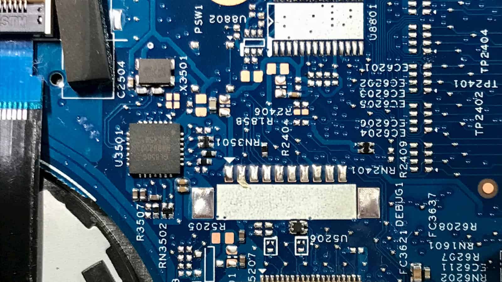
What is a Printed Circuit Board (PCB)?
A printed circuit board (PCB) is a flat board made of insulating material, such as fiberglass or composite epoxy, with conductive pathways etched or printed onto its surface. These pathways, also known as traces, connect various electronic components mounted on the board, forming a complete electronic circuit. PCBs are the foundation of most modern electronic devices, ranging from smartphones and computers to medical equipment and aerospace systems.
The Importance of Testing in PCB Manufacturing
Testing is an integral part of the PCB manufacturing process, as it ensures the quality, reliability, and functionality of the final product. Without proper testing, defective PCBs can lead to device malfunctions, poor performance, and even safety hazards. Some of the common issues that can arise in PCB manufacturing include:
- Shorts: Unintended connections between two or more points on the PCB
- Opens: Missing or broken connections between points on the PCB
- Component failures: Defective or incorrectly placed components
- Incorrect values: Components with wrong values or tolerances
Testing helps identify these issues early in the manufacturing process, allowing for timely corrections and reducing the risk of defective products reaching the end-users.
What is In-Circuit Testing (ICT)?
In-Circuit Testing (ICT) is an automated testing method that verifies the functionality of individual components and their interconnections on a PCB assembly. It is performed using a specialized ICT fixture, which consists of a bed of nails that makes contact with specific test points on the PCB. The test points are usually designed into the PCB layout to facilitate ICT.
During the ICT process, the fixture applies electrical signals to the test points and measures the response, comparing it to the expected values. This allows the system to detect various faults, such as shorts, opens, incorrect component values, and missing or incorrectly placed components.

The ICT Process
The ICT process typically involves the following steps:
-
Test Program Generation: A test program is created based on the PCB design data, including the schematic, bill of materials (BOM), and layout. The program defines the test points, expected values, and test sequences.
-
Fixture Design and Fabrication: An ICT fixture is designed and fabricated to match the specific PCB layout. The fixture includes a bed of nails that aligns with the test points on the PCB.
-
PCB Loading: The PCB assembly is loaded into the ICT fixture, ensuring proper alignment and contact between the test points and the bed of nails.
-
Testing: The ICT system applies electrical signals to the test points and measures the response, comparing it to the expected values defined in the test program. The system flags any discrepancies as faults.
-
Fault Diagnosis: If faults are detected, the ICT system provides information about the type and location of the faults, allowing for further diagnosis and repair.
-
Repair and Retest: Faulty PCBs are removed from the fixture, repaired, and retested to ensure they meet the required specifications.
Advantages of In-Circuit Testing
ICT offers several advantages over other testing methods, such as functional testing or flying probe testing:
-
High Fault Coverage: ICT can detect a wide range of faults, including shorts, opens, incorrect component values, and missing or incorrectly placed components. This comprehensive fault coverage helps ensure the quality and reliability of the PCB assembly.
-
Speed: ICT is a fast testing method, as it can test multiple points on the PCB simultaneously. This high-speed testing enables manufacturers to achieve higher production throughput and reduce overall testing time.
-
Early Fault Detection: ICT is typically performed early in the manufacturing process, often immediately after PCB assembly. This allows for the early detection and correction of faults, reducing the risk of defective products progressing further down the production line.
-
Automated Process: ICT is a fully automated testing process, minimizing the need for human intervention and reducing the risk of human error. This automation also contributes to the high speed and consistency of the testing process.
-
Detailed Fault Diagnosis: ICT systems provide detailed information about detected faults, including the type and location of the fault. This information facilitates efficient repair and troubleshooting, reducing repair time and costs.
Limitations of In-Circuit Testing
While ICT is a powerful and widely used testing method, it does have some limitations:
-
Test Point Access: ICT requires physical access to test points on the PCB. This means that the PCB layout must be designed with test points in mind, which can increase the PCB size and complexity. In some cases, test points may be difficult or impossible to access due to the PCB design or component placement.
-
Fixture Cost: ICT requires a custom-designed fixture for each unique PCB layout. The design and fabrication of these fixtures can be costly, especially for low-volume production runs or frequently changing PCB designs.
-
Limited Functional Testing: ICT primarily focuses on testing individual components and their interconnections. It does not provide comprehensive functional testing of the entire PCB assembly. Functional testing is often performed separately to ensure the overall performance and functionality of the product.
-
Component Tolerance: ICT relies on measuring electrical characteristics of components and comparing them to expected values. Components with wide tolerances or variable characteristics, such as some analog components, may be difficult to test accurately using ICT.
Combining ICT with Other Testing Methods
To overcome the limitations of ICT and ensure comprehensive testing of PCB assemblies, manufacturers often combine ICT with other testing methods, such as:
-
Functional Testing: Functional testing verifies the overall performance and functionality of the PCB assembly by simulating real-world operating conditions. It ensures that the product meets its intended specifications and functions correctly as a complete system.
-
Boundary Scan Testing: Boundary scan testing, also known as JTAG testing, is a method that uses a special test access port (TAP) to test the interconnections between digital components on a PCB. It complements ICT by providing access to components that may be difficult to test using physical test points.
-
Flying Probe Testing: Flying probe testing uses movable test probes to make contact with test points on the PCB. It offers greater flexibility than ICT, as it does not require a custom fixture. However, flying probe testing is generally slower than ICT and may not provide the same level of fault coverage.
By combining these testing methods, manufacturers can ensure a high level of quality and reliability in their PCB assemblies.
Frequently Asked Questions (FAQ)
-
Q: What is the difference between ICT and functional testing?
A: ICT focuses on testing individual components and their interconnections, while functional testing verifies the overall performance and functionality of the PCB assembly under real-world operating conditions. -
Q: Can ICT detect all types of faults in a PCB assembly?
A: ICT can detect a wide range of faults, including shorts, opens, incorrect component values, and missing or incorrectly placed components. However, it may not detect all types of faults, such as those related to component tolerance or functional issues. -
Q: Is ICT necessary for all PCB assemblies?
A: The decision to use ICT depends on factors such as the complexity of the PCB, the production volume, and the required level of quality and reliability. In some cases, other testing methods may be sufficient or more cost-effective. -
Q: How long does ICT take?
A: The duration of ICT depends on the complexity of the PCB and the number of test points. However, ICT is generally a fast testing method, as it can test multiple points simultaneously. Typical test times range from a few seconds to a few minutes per PCB. -
Q: Can ICT be performed on populated PCBs?
A: Yes, ICT is typically performed on fully populated PCBs, after the components have been soldered onto the board. This allows for the testing of both the components and their interconnections.
Conclusion
In-Circuit Testing (ICT) is a crucial process in the manufacturing of printed circuit boards (PCBs), ensuring the quality, reliability, and functionality of the final product. By verifying the functionality of individual components and their interconnections, ICT helps detect and correct faults early in the production process, reducing the risk of defective products reaching end-users.
While ICT offers numerous advantages, such as high fault coverage, speed, and early fault detection, it also has limitations, such as the need for test point access and custom fixtures. To overcome these limitations and ensure comprehensive testing, manufacturers often combine ICT with other testing methods, such as functional testing, boundary scan testing, and flying probe testing.
As PCBs continue to grow in complexity and the demand for high-quality electronic products increases, the role of ICT in PCB manufacturing will remain essential. By understanding the principles, processes, and advantages of ICT, manufacturers can optimize their testing strategies and deliver reliable, high-performance products to their customers.
| Testing Method | Advantages | Limitations |
|---|---|---|
| In-Circuit Testing (ICT) | – High fault coverage – Speed – Early fault detection – Automated process – Detailed fault diagnosis |
– Requires test point access – Custom fixture cost – Limited functional testing – Difficulty testing components with wide tolerances |
| Functional Testing | – Verifies overall performance and functionality – Simulates real-world operating conditions |
– May not detect all component-level faults – Slower than ICT |
| Boundary Scan Testing | – Tests interconnections between digital components – Provides access to components difficult to test with physical test points |
– Limited to digital components with boundary scan architecture – May require additional hardware and software |
| Flying Probe Testing | – Flexible, does not require custom fixtures – Can test a wide variety of PCBs |
– Slower than ICT – May not provide the same level of fault coverage as ICT |
In summary, ICT is a valuable tool in the PCB manufacturing process, offering high fault coverage, speed, and early fault detection. When combined with other testing methods, ICT helps ensure the production of high-quality, reliable PCB assemblies that meet the ever-growing demands of the electronics industry.


Leave a Reply