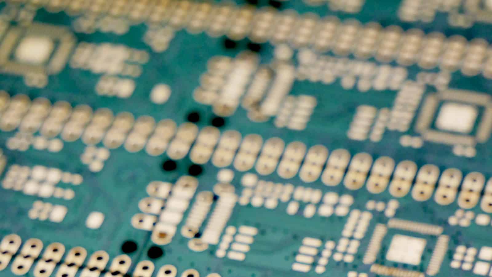
What is ENIG Finish?
ENIG finish is a type of surface finish applied to PCBs that consists of a layer of nickel followed by a thin layer of gold. The nickel layer provides a barrier between the copper substrate and the gold layer, preventing the formation of intermetallic compounds that can degrade solderability over time. The gold layer provides excellent oxidation resistance and ensures good solderability.
Advantages of ENIG Finish
ENIG finish offers several advantages over other surface finishes, including:
- Excellent solderability
- Good oxidation resistance
- Long shelf life
- Compatibility with a wide range of soldering processes
- Suitable for fine-pitch components
- Aesthetically pleasing appearance
Applications of ENIG Finish PCBs
ENIG finish PCBs are widely used in various industries, including:
- Aerospace and defense
- Automotive
- Medical devices
- Telecommunications
- Consumer electronics
The ENIG Plating Process
The ENIG plating process involves several steps to ensure a high-quality surface finish. The process can be broken down into the following stages:
1. Cleaning and Preparation
Before the ENIG plating process can begin, the PCB must be thoroughly cleaned to remove any contaminants or oxidation. This is typically done using a combination of chemical cleaning agents and mechanical cleaning processes, such as brushing or ultrasonic cleaning.
2. Nickel Plating
Once the PCB is clean, it is immersed in an electroless nickel plating solution. This solution contains nickel ions and a reducing agent that causes the nickel to deposit onto the copper surface of the PCB. The nickel layer is typically between 3 and 6 microns thick and provides a barrier between the copper and the gold layer.
3. Gold Plating
After the nickel plating is complete, the PCB is immersed in an immersion gold plating solution. This solution contains gold ions that deposit onto the nickel surface, forming a thin layer of gold typically between 0.05 and 0.2 microns thick. The gold layer provides excellent oxidation resistance and ensures good solderability.
4. Rinsing and Drying
Once the gold plating is complete, the PCB is rinsed with deionized water to remove any excess plating solution and then dried using hot air or infrared lamps.
Comparing ENIG to Other Surface Finishes
ENIG is just one of several surface finishes available for PCBs. Other popular surface finishes include:
- HASL (Hot Air Solder Leveling)
- OSP (Organic Solderability Preservative)
- Immersion Silver
- Immersion Tin
Each surface finish has its own advantages and disadvantages, as summarized in the table below:
| Surface Finish | Advantages | Disadvantages |
|---|---|---|
| ENIG | Excellent solderability, long shelf life, suitable for fine-pitch components | Higher cost, more complex process |
| HASL | Low cost, good solderability | Uneven surface, not suitable for fine-pitch components |
| OSP | Low cost, flat surface | Limited shelf life, not suitable for multiple reflow cycles |
| Immersion Silver | Good solderability, flat surface | Limited shelf life, can tarnish over time |
| Immersion Tin | Good solderability, low cost | Limited shelf life, can form whiskers |

Designing for ENIG Finish PCBs
When designing PCBs for ENIG finish, there are several factors to consider to ensure the best possible results:
1. Copper Thickness
The copper thickness of the PCB should be sufficient to ensure good adhesion of the nickel and gold layers. A minimum copper thickness of 18 microns is recommended for ENIG finish PCBs.
2. Trace Width and Spacing
The trace width and spacing should be designed to accommodate the ENIG plating process. A minimum trace width of 0.1 mm and a minimum spacing of 0.1 mm are recommended to ensure good coverage and avoid bridging between traces.
3. Soldermask Design
The soldermask design should be optimized for ENIG finish PCBs. The soldermask should be designed with sufficient clearance around the pads to ensure good coverage of the nickel and gold layers. A minimum soldermask clearance of 0.05 mm is recommended.
4. Pad Size and Shape
The pad size and shape should be designed to ensure good solderability and reliability. A minimum pad size of 0.5 mm is recommended for ENIG finish PCBs. The pad shape should be designed to minimize the risk of solder bridging and ensure good solder joint formation.
Quality Control for ENIG Finish PCBs
To ensure the highest quality ENIG finish PCBs, several quality control measures should be implemented throughout the manufacturing process:
1. Plating Thickness Measurement
The thickness of the nickel and gold layers should be measured regularly to ensure they meet the specified requirements. X-ray fluorescence (XRF) is commonly used to measure the thickness of the plating layers.
2. Visual Inspection
Visual inspection should be performed to check for any defects or irregularities in the ENIG finish, such as nodules, pits, or discoloration.
3. Solderability Testing
Solderability testing should be performed to ensure the ENIG finish PCBs meet the required solderability standards. The most common solderability test methods include the wetting balance test and the dip-and-look test.
4. Adhesion Testing
Adhesion testing should be performed to ensure the nickel and gold layers adhere properly to the copper substrate. The most common adhesion test method is the tape test, where a piece of adhesive tape is applied to the surface of the PCB and then peeled off to check for any lifting or delamination of the plating layers.
Frequently Asked Questions (FAQ)
- What is the typical thickness of the nickel and gold layers in ENIG finish PCBs?
-
The typical thickness of the nickel layer is between 3 and 6 microns, while the typical thickness of the gold layer is between 0.05 and 0.2 microns.
-
How does ENIG finish compare to HASL in terms of cost?
-
ENIG finish is generally more expensive than HASL due to the more complex plating process and the use of gold. However, the higher cost is often justified by the superior solderability and reliability of ENIG finish PCBs.
-
Can ENIG finish PCBs be used for high-temperature applications?
-
Yes, ENIG finish PCBs are suitable for high-temperature applications due to the excellent thermal stability of the nickel and gold layers. However, the maximum operating temperature will depend on the specific PCB design and the components used.
-
How long is the shelf life of ENIG finish PCBs?
-
ENIG finish PCBs have a typical shelf life of 12 to 24 months, depending on the storage conditions. Proper storage in a cool, dry environment can help extend the shelf life of ENIG finish PCBs.
-
Are there any environmental concerns with ENIG plating?
- The ENIG plating process does involve the use of chemicals that can be harmful to the environment if not properly managed. However, responsible PCB manufacturers will have proper waste management and disposal procedures in place to minimize the environmental impact of the ENIG plating process.
Conclusion
ENIG finish PCBs offer a high-quality surface finish that provides excellent solderability, durability, and shelf life. The combination of a nickel barrier layer and a thin gold surface layer ensures good oxidation resistance and compatibility with a wide range of soldering processes. While ENIG finish may be more expensive than some other surface finishes, the superior performance and reliability make it a popular choice for many applications, particularly in industries such as aerospace, automotive, and medical devices.
When designing PCBs for ENIG finish, it is important to consider factors such as copper thickness, trace width and spacing, soldermask design, and pad size and shape to ensure the best possible results. Quality control measures such as plating thickness measurement, visual inspection, solderability testing, and adhesion testing should also be implemented to ensure the highest quality ENIG finish PCBs.
Overall, ENIG finish PCBs provide a reliable and high-performance solution for a wide range of applications, and their popularity is likely to continue to grow as demand for high-quality PCBs increases in various industries.


Leave a Reply