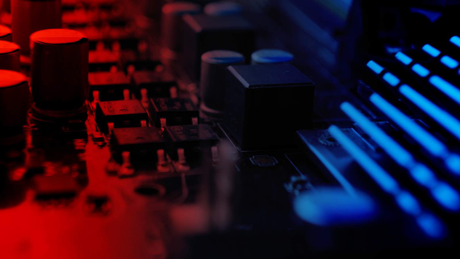
Overview of Electronic Component Manufacturing
Electronic component manufacturing involves a wide range of processes and technologies, including:
- Semiconductor fabrication
- Printed circuit board (PCB) manufacturing
- Passive component manufacturing
- Electromechanical component manufacturing
- Assembly and packaging
Each of these areas requires specialized expertise, equipment, and materials to produce high-quality, reliable components that meet the demanding requirements of modern electronic devices.
Semiconductor Fabrication
Semiconductors, such as transistors and integrated circuits, are the foundation of modern electronics. The manufacturing process for semiconductors is highly complex and involves multiple steps, including:
- Wafer production
- Photolithography
- Etching
- Doping
- Metallization
- Packaging
Semiconductor fabrication is carried out in specialized facilities called foundries or fabs, which maintain ultra-clean environments to prevent contamination of the delicate devices.
Wafer Production
The first step in semiconductor manufacturing is the production of wafers, which are thin, circular slices of single-crystal semiconductor material, typically silicon. Wafers are grown from a seed crystal in a process called Czochralski growth, which involves slowly pulling a single crystal from a melt of pure silicon.
Photolithography
Photolithography is the process of transferring a pattern onto the wafer surface using light-sensitive chemicals called photoresists. The pattern represents the various layers and features of the semiconductor device, such as transistors and interconnects.
Etching
After the photoresist pattern is developed, the exposed areas of the wafer are etched away using chemical or plasma etching processes. This selectively removes material to create the desired features on the wafer surface.
Doping
Doping involves introducing impurities into the semiconductor material to modify its electrical properties. This is typically done through ion implantation or diffusion processes, which allow precise control over the concentration and distribution of dopants in the wafer.
Metallization
Metallization is the process of depositing metal layers onto the wafer surface to create interconnects between different components of the semiconductor device. This is typically done through physical vapor deposition (PVD) or chemical vapor deposition (CVD) processes.
Packaging
Once the semiconductor devices are fabricated on the wafer, they must be packaged to protect them from damage and facilitate their integration into electronic systems. Packaging involves dicing the wafer into individual chips, attaching them to a substrate or leadframe, and encapsulating them in a protective material, such as ceramic or plastic.
Printed Circuit Board (PCB) Manufacturing
Printed circuit boards (PCBs) are the backbone of most electronic devices, providing a platform for mounting and interconnecting various components. PCB manufacturing involves several key steps:
- Design and layout
- Material selection
- Fabrication
- Assembly
PCB Design and Layout
PCB design involves creating a schematic representation of the electronic circuit and translating it into a physical layout that specifies the location and routing of components and traces on the board. This process is typically done using computer-aided design (CAD) software.
Material Selection
PCBs can be made from a variety of materials, depending on the specific requirements of the application. The most common base material for PCBs is FR-4, a glass-reinforced epoxy laminate. Other materials, such as polyimide or PTFE, may be used for high-frequency or high-temperature applications.
PCB Fabrication
PCB fabrication involves a series of steps to create the conductive traces and features on the board:
- Copper clad laminate: The base material is coated with a thin layer of copper on one or both sides.
- Drilling: Holes are drilled through the board to accommodate through-hole components and vias.
- Patterning: The desired circuit pattern is transferred onto the copper layer using photolithography and etching processes similar to those used in semiconductor manufacturing.
- Plating: Additional copper is plated onto the traces and through-holes to improve conductivity and durability.
- Solder mask application: A protective layer of polymer is applied over the board, leaving only the areas to be soldered exposed.
- Silkscreen: Text and symbols are printed onto the board surface to aid in assembly and identification.
PCB Assembly
PCB assembly involves mounting and soldering components onto the fabricated board. This can be done manually for low-volume or prototype production, but is typically automated using pick-and-place machines and reflow soldering processes for high-volume manufacturing.
Passive Component Manufacturing
Passive components, such as resistors, capacitors, and inductors, are essential elements in electronic circuits. These components are manufactured using a variety of processes, depending on the specific type and requirements of the component.
Resistor Manufacturing
Resistors are manufactured using several different technologies, including:
- Carbon composition: A mixture of carbon and binder is molded into a cylindrical shape and fitted with wire leads.
- Carbon film: A thin film of carbon is deposited onto a ceramic substrate and laser-trimmed to achieve the desired resistance value.
- Metal film: A thin film of metal, such as nickel-chromium, is deposited onto a ceramic substrate and laser-trimmed.
- Wirewound: A wire made of a resistive alloy is wound around a ceramic or fiberglass core.
Capacitor Manufacturing
Capacitors are manufactured using various dielectric materials and electrode configurations, depending on the desired capacitance and voltage rating. Some common types of capacitors include:
- Ceramic: Alternating layers of ceramic dielectric and metal electrodes are stacked and sintered to form a monolithic block.
- Film: A thin film of plastic dielectric, such as polyester or polypropylene, is wound between two metal foil electrodes.
- Electrolytic: A metal foil anode and a conductive electrolyte are separated by an oxide layer that acts as the dielectric.
Inductor Manufacturing
Inductors are typically manufactured by winding a wire around a core material, such as ferrite or iron powder. The wire can be wound in various patterns, such as solenoid, toroid, or multilayer, to achieve the desired inductance and frequency response.
Electromechanical Component Manufacturing
Electromechanical components, such as switches, relays, and connectors, are essential for interfacing between electronic circuits and the physical world. These components are manufactured using a combination of mechanical and electrical processes.
Switch and Relay Manufacturing
Switches and relays are manufactured using a variety of technologies, including:
- Snap-action: A curved metal blade snaps between two contacts when actuated by a button or lever.
- Reed: Two ferromagnetic reeds are sealed in a glass envelope and actuated by an external magnetic field.
- Solid-state: Semiconductor devices, such as transistors or thyristors, are used to switch current electronically.
Connector Manufacturing
Connectors are manufactured using a combination of stamping, molding, and plating processes:
- Stamping: Metal contacts are stamped from a sheet of copper alloy or other conductive material.
- Molding: The insulating housing of the connector is molded from plastic or other dielectric material.
- Plating: The contacts are plated with gold, silver, or tin to improve conductivity and corrosion resistance.
- Assembly: The contacts are inserted into the housing and retained by features such as barbs or lances.
Assembly and Packaging
After individual components are manufactured, they must be assembled into functional modules or complete devices. This involves several processes, such as:
- Surface mount assembly: Components are mounted onto PCBs using automated pick-and-place machines and soldered using reflow or wave soldering processes.
- Through-hole assembly: Components with wire leads are inserted into holes in the PCB and soldered in place.
- Wire bonding: Bare semiconductor die are attached to a substrate or leadframe and connected to the package leads using fine gold or aluminum wires.
- Encapsulation: The assembled components are encapsulated in a protective material, such as epoxy or silicone, to provide mechanical support and environmental protection.
Challenges in Electronic Component Manufacturing
Electronic component manufacturing faces several challenges, including:
- Miniaturization: As electronic devices become smaller and more complex, components must be manufactured with ever-increasing precision and density.
- Performance: Demands for higher speed, lower power consumption, and improved reliability require continuous innovation in materials, processes, and designs.
- Cost: Competitive pressures drive manufacturers to reduce costs through automation, process optimization, and supply chain management.
- Environmental concerns: Regulations on hazardous substances, such as lead and cadmium, require manufacturers to adopt new materials and processes that are more environmentally friendly.
Future Trends in Electronic Component Manufacturing
The future of electronic component manufacturing will be shaped by several key trends, including:
- Advanced packaging: Techniques such as 3D integration, wafer-level packaging, and system-in-package (SiP) will enable higher density and performance.
- Flexible and printed electronics: New materials and processes will enable the production of electronic components on flexible substrates, such as plastic or paper.
- Additive manufacturing: 3D printing technologies will allow the rapid prototyping and production of complex, customized electronic components.
- Smart manufacturing: The integration of advanced sensors, data analytics, and artificial intelligence will enable more efficient, agile, and responsive manufacturing processes.

FAQs
What are the most common materials used in electronic component manufacturing?
The most common materials used in electronic component manufacturing include:
- Silicon: The primary material used in semiconductor devices.
- Copper: Used for conductive traces on PCBs and leadframes.
- Aluminum: Used for interconnects in integrated circuits and for electrolytic capacitor anodes.
- Ceramic: Used as a substrate material for PCBs and as a dielectric in capacitors.
- Plastic: Used for PCB substrates, connector housings, and component encapsulation.
What is the difference between through-hole and surface mount components?
Through-hole components have wire leads that are inserted into holes drilled in the PCB and soldered in place. Surface mount components are mounted directly onto the surface of the PCB and soldered using a reflow or wave soldering process. Surface mount components are generally smaller and more suitable for high-density designs, while through-hole components are more robust and easier to replace.
What is the role of cleanrooms in electronic component manufacturing?
Cleanrooms are controlled environments with low levels of airborne particulates, which are essential for many electronic component manufacturing processes, particularly semiconductor fabrication. Cleanrooms prevent contamination of sensitive materials and devices, which can cause defects, performance issues, or reliability problems.
What are the main steps in the semiconductor fabrication process?
The main steps in the semiconductor fabrication process are:
- Wafer production: Growing a single crystal of silicon and slicing it into thin wafers.
- Photolithography: Transferring a pattern onto the wafer surface using light-sensitive chemicals.
- Etching: Selectively removing material from the wafer surface to create features.
- Doping: Introducing impurities into the silicon to modify its electrical properties.
- Metallization: Depositing metal layers to create interconnects between components.
- Packaging: Dicing the wafer into individual chips and encapsulating them in a protective package.
What are some of the key challenges facing the electronic component manufacturing industry?
Some of the key challenges facing the electronic component manufacturing industry include:
- Miniaturization: Producing ever-smaller components with higher precision and density.
- Performance: Meeting demands for higher speed, lower power consumption, and improved reliability.
- Cost: Reducing manufacturing costs through automation, process optimization, and supply chain management.
- Environmental concerns: Complying with regulations on hazardous substances and adopting more environmentally friendly materials and processes.
In conclusion, electronic component manufacturing is a complex and multifaceted industry that plays a crucial role in the production of modern electronic devices. From semiconductors and PCBs to passive and electromechanical components, the manufacturing processes involved require specialized expertise, equipment, and materials. As electronic devices continue to evolve and become more sophisticated, the electronic component manufacturing industry will need to adapt and innovate to meet the challenges of miniaturization, performance, cost, and environmental sustainability.


Leave a Reply