Table of Contents
- Introduction to Inverter PCBs
- Types of Inverter PCBs
- Half-Bridge Inverter PCB
- Full-Bridge Inverter PCB
- Three-Phase Inverter PCB
- Multilevel Inverter PCB
- Key Components of an Inverter PCB
- Power Switches
- Gate Drivers
- Capacitors and Inductors
- Sensors and Protection Circuits
- Inverter PCB Design Considerations
- Power Rating and Efficiency
- Thermal Management
- EMI and Noise Reduction
- Component Selection and Placement
- Applications of Inverter PCBs
- Solar Power Systems
- Electric Vehicles
- Uninterruptible Power Supplies (UPS)
- Variable Frequency Drives (VFDs)
- Inverter PCB Manufacturing Process
- PCB Material Selection
- PCB Layering and Routing
- Component Soldering and Assembly
- Testing and Quality Control
- Future Trends in Inverter PCB Technology
- Wide Bandgap Semiconductors
- Digital Power Management
- High-Frequency Inverters
- Advanced Packaging Techniques
- Frequently Asked Questions (FAQ)
- Conclusion
Introduction to Inverter PCBs
An inverter is a power electronic device that converts DC power to AC power at a desired frequency and voltage level. The heart of an inverter is the inverter PCB, which contains the necessary components and circuitry to perform the DC-to-AC conversion. Inverter PCBs are designed to handle high power levels, operate efficiently, and provide reliable performance in various environmental conditions.
The basic working principle of an inverter involves using power switches, such as IGBTs or MOSFETs, to rapidly switch the DC input on and off, creating a pulsating DC waveform. This pulsating waveform is then filtered and smoothed to produce a sinusoidal AC output. The frequency and voltage of the AC output can be controlled by adjusting the switching frequency and duty cycle of the power switches.
Types of Inverter PCBs
There are several types of inverter PCBs, each with its own unique circuit topology and application. The most common types include:
Half-Bridge Inverter PCB
A half-bridge inverter PCB consists of two power switches and two capacitors. The switches are connected in series across the DC input, and the capacitors are used to divide the DC voltage in half. By alternately turning the switches on and off, the inverter produces a square wave AC output. Half-bridge inverters are simple and cost-effective, making them suitable for low-power applications.
Full-Bridge Inverter PCB
A full-bridge inverter PCB uses four power switches arranged in two legs, forming an H-bridge configuration. Each leg of the H-bridge consists of two switches connected in series across the DC input. By controlling the switching sequence of the four switches, the inverter can produce a full-wave AC output. Full-bridge inverters offer higher power output and efficiency compared to half-bridge inverters, making them popular in medium to high-power applications.
Three-Phase Inverter PCB
A three-phase inverter PCB is used to generate three-phase AC power, which is commonly used in industrial and commercial applications. It consists of three half-bridge or full-bridge inverter circuits, each producing a single phase of the AC output. The three phases are electrically separated by 120 degrees, resulting in a balanced three-phase system. Three-phase inverters are essential in applications such as motor drives, wind turbines, and large-scale solar power systems.
Multilevel Inverter PCB
Multilevel inverter PCBs are designed to produce AC outputs with multiple voltage levels, resulting in a staircase-like waveform that closely approximates a sinusoidal wave. The most common types of multilevel inverters are diode-clamped, capacitor-clamped, and cascaded H-bridge inverters. Multilevel inverters offer several advantages, including reduced harmonic distortion, lower electromagnetic interference (EMI), and higher power quality. However, they are more complex and expensive compared to traditional two-level inverters.
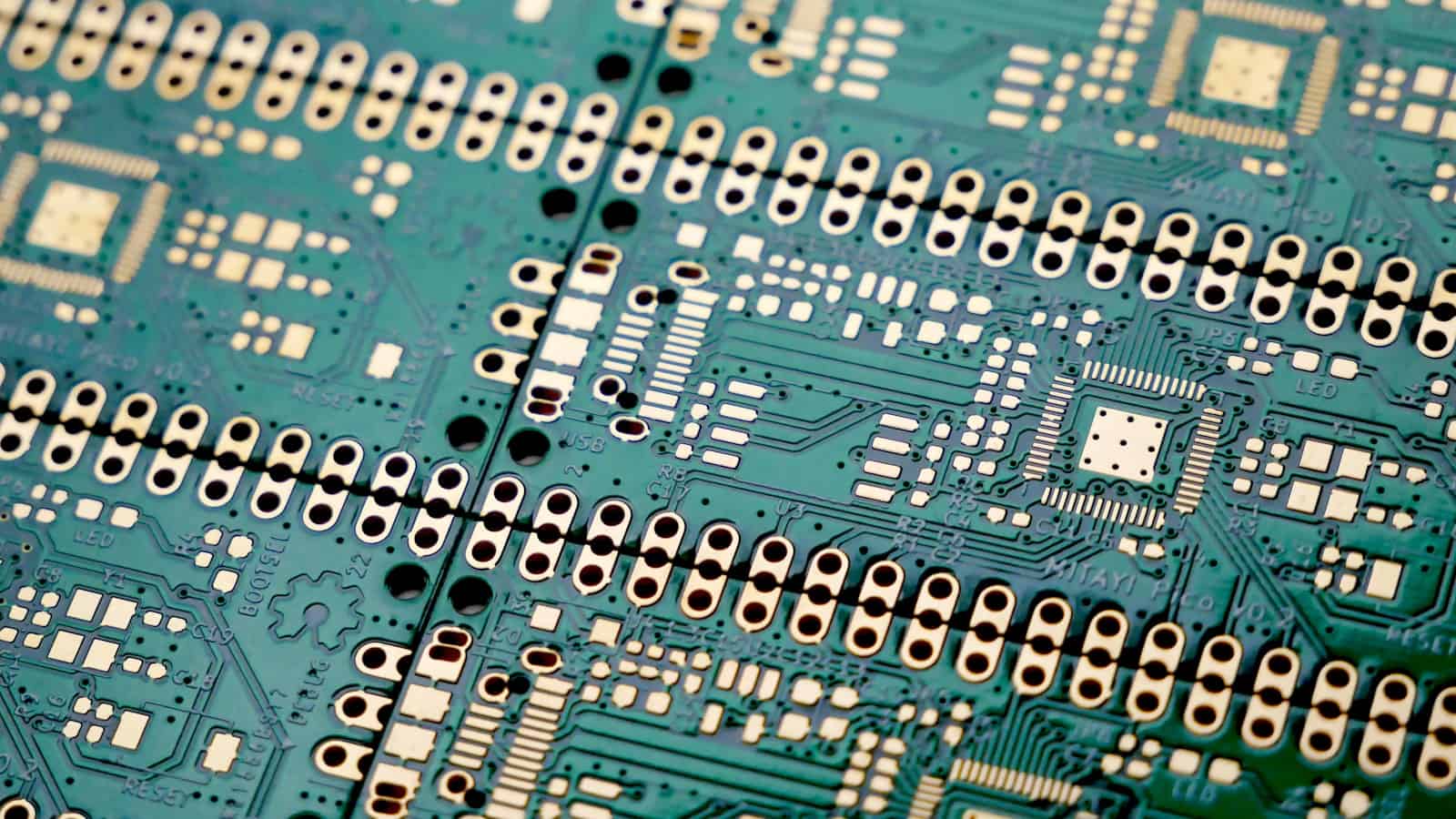
Key Components of an Inverter PCB
An inverter PCB consists of several key components that work together to perform the DC-to-AC conversion. These components include:
Power Switches
Power switches are the backbone of an inverter PCB, responsible for rapidly switching the DC input on and off to create the pulsating waveform. The most commonly used power switches in inverters are Insulated Gate Bipolar Transistors (IGBTs) and Metal-Oxide-Semiconductor Field-Effect Transistors (MOSFETs). IGBTs are preferred for high-power applications due to their high current handling capability and low on-state voltage drop, while MOSFETs are favored in low to medium-power applications for their fast switching speeds and low gate drive requirements.
Gate Drivers
Gate drivers are essential components in an inverter PCB, responsible for controlling the switching of the power switches. They provide the necessary voltage and current to charge and discharge the gate capacitance of the power switches, ensuring fast and reliable switching. Gate drivers also provide electrical isolation between the low-voltage control circuitry and the high-voltage power stage, protecting the sensitive control components from voltage spikes and transients.
Capacitors and Inductors
Capacitors and inductors are used in inverter PCBs for energy storage, filtering, and smoothing of the pulsating waveform. Capacitors are employed to store energy during the off-state of the power switches and provide a low-impedance path for high-frequency currents. They also help to reduce voltage ripple and maintain a stable DC link voltage. Inductors, on the other hand, are used to filter out high-frequency harmonics and smooth the AC output waveform.
Sensors and Protection Circuits
Inverter PCBs incorporate various sensors and protection circuits to ensure safe and reliable operation. Current and voltage sensors monitor the input and output parameters of the inverter, providing feedback to the control system for regulation and protection purposes. Overcurrent, overvoltage, and temperature protection circuits are implemented to detect fault conditions and take appropriate actions, such as shutting down the inverter or limiting the output current, to prevent damage to the components and ensure user safety.
Inverter PCB Design Considerations
Designing an inverter PCB requires careful consideration of several factors to ensure optimal performance, reliability, and safety. Some of the key design considerations include:
Power Rating and Efficiency
The power rating of an inverter PCB determines its maximum output power capability. Designers must select components and design the PCB layout to handle the required power levels efficiently. High-efficiency inverters minimize power losses, reduce heat generation, and improve overall system performance. Efficiency can be optimized through the selection of low-loss components, proper PCB layout, and the use of advanced control techniques such as soft switching and power factor correction.
Thermal Management
Inverter PCBs generate significant heat during operation due to power losses in the components. Effective thermal management is crucial to prevent overheating and ensure reliable operation. Designers must consider the thermal characteristics of the components, the PCB material, and the operating environment when designing the inverter PCB. Thermal management techniques include the use of heat sinks, thermal interface materials, and forced air or liquid cooling systems. Proper component placement and PCB layout also play a vital role in heat dissipation and temperature distribution.
EMI and Noise Reduction
Inverter PCBs generate high-frequency switching noise and electromagnetic interference (EMI) that can affect nearby electronic devices and cause compliance issues with electromagnetic compatibility (EMC) regulations. Designers must implement noise reduction techniques to minimize EMI and ensure the inverter meets the required EMC standards. Common noise reduction techniques include the use of snubber circuits, filters, shielding, and proper grounding. PCB layout techniques, such as minimizing loop areas, using ground planes, and separating sensitive signals from noisy power traces, also contribute to noise reduction.
Component Selection and Placement
The selection and placement of components on an inverter PCB have a significant impact on its performance, reliability, and manufacturability. Designers must choose components that meet the electrical, thermal, and mechanical requirements of the application. Factors such as voltage and current ratings, switching speeds, package types, and cost should be considered when selecting components. Proper component placement is essential to minimize parasitic inductances and capacitances, reduce EMI, and optimize heat dissipation. Designers should also consider the manufacturing aspects, such as component availability, solderability, and assembly tolerances, to ensure the inverter PCB can be efficiently manufactured and assembled.
Applications of Inverter PCBs
Inverter PCBs find applications in a wide range of power electronic systems across various industries. Some of the most common applications include:
Solar Power Systems
Inverter PCBs are an essential component in solar power systems, converting the DC power generated by solar panels into AC power suitable for grid integration or local consumption. Solar inverters can be classified into three main types: string inverters, microinverters, and central inverters. String inverters are connected to a series of solar panels, while microinverters are dedicated to individual solar panels. Central inverters are used in large-scale solar power plants, handling the combined power output of multiple solar arrays.
Electric Vehicles
Inverter PCBs play a crucial role in electric vehicle (EV) powertrains, converting the DC power from the battery pack to AC power for driving the electric motors. EV inverters must handle high power levels, typically in the range of tens to hundreds of kilowatts, and operate efficiently to maximize the driving range and performance of the vehicle. They also need to be compact, lightweight, and reliable to meet the stringent requirements of automotive applications.
Uninterruptible Power Supplies (UPS)
Uninterruptible power supplies (UPS) rely on inverter PCBs to provide backup AC power during power outages or disturbances. UPS inverters convert the DC power from batteries or other energy storage systems into clean and stable AC power to keep critical loads, such as computers, servers, and medical equipment, running without interruption. UPS inverters must have fast response times, low harmonic distortion, and high reliability to ensure the continuity and quality of the power supply.
Variable Frequency Drives (VFDs)
Variable frequency drives (VFDs) use inverter PCBs to control the speed and torque of AC motors in industrial applications. VFDs convert the fixed-frequency AC input power to a variable-frequency AC output, allowing precise control of motor speed and torque. This enables energy savings, improved process control, and reduced mechanical stress on the motor and driven equipment. VFD inverters must be rugged, reliable, and capable of operating in harsh industrial environments.
Inverter PCB Manufacturing Process
The manufacturing process of an inverter PCB involves several stages, each critical to ensuring the quality and reliability of the final product. The main steps in the inverter PCB manufacturing process include:
PCB Material Selection
The choice of PCB material is crucial in inverter applications, as it must provide the necessary electrical, thermal, and mechanical properties. Common PCB materials for inverters include FR-4, high-Tg FR-4, and metal-core PCBs. FR-4 is a cost-effective and widely used material, suitable for general-purpose inverters. High-Tg FR-4 offers improved thermal stability and is preferred in high-temperature applications. Metal-core PCBs, such as aluminum or copper-based substrates, provide excellent thermal conductivity and are used in high-power inverters that require efficient heat dissipation.
PCB Layering and Routing
Inverter PCBs often require multiple layers to accommodate the complex circuitry and provide necessary power and signal routing. The number of layers depends on the complexity of the inverter design and the power level it handles. Designers must carefully plan the layer stack-up and routing to minimize signal integrity issues, reduce EMI, and ensure proper current handling capacity. Power and ground planes are used to provide low-impedance paths for high-frequency currents and minimize voltage drops. Signal traces are routed to minimize crosstalk and maintain the required impedance.
Component Soldering and Assembly
The component soldering and assembly process involves mounting the various components onto the inverter PCB. Surface mount technology (SMT) is widely used in inverter PCB assembly due to its high precision, automation, and space-saving advantages. The SMT process involves applying solder paste to the PCB pads, placing the components using pick-and-place machines, and reflowing the solder in a controlled oven. Through-hole components, such as large capacitors and connectors, are inserted and soldered manually or using wave soldering techniques. Proper soldering and assembly are essential to ensure reliable electrical connections and mechanical stability of the components.
Testing and Quality Control
Thorough testing and quality control are critical in inverter PCB manufacturing to ensure the functionality, performance, and reliability of the final product. Various tests are performed at different stages of the manufacturing process, including:
- In-circuit testing (ICT): Verifies the proper connection and functionality of individual components on the PCB.
- Functional testing: Checks the overall functionality of the inverter PCB under different operating conditions and load scenarios.
- Burn-in testing: Subjects the inverter PCB to elevated temperatures and power cycles to identify early-life failures and ensure reliability.
- Hipot testing: Applies high voltage to the inverter PCB to test the insulation and dielectric strength of the components and PCB material.
- EMC testing: Measures the electromagnetic emissions and immunity of the inverter PCB to ensure compliance with relevant EMC standards.
Quality control measures, such as visual inspection, X-ray inspection, and automated optical inspection (AOI), are employed to detect manufacturing defects, such as solder bridges, component misalignment, and missing components.
Future Trends in Inverter PCB Technology
Inverter PCB technology continues to evolve, driven by the increasing demand for higher power density, efficiency, and reliability in power electronic applications. Some of the future trends in inverter PCB technology include:
Wide Bandgap Semiconductors
Wide bandgap (WBG) semiconductors, such as silicon carbide (SiC) and gallium nitride (GaN), are emerging as promising alternatives to traditional silicon-based power switches. WBG devices offer higher breakdown voltage, faster switching speeds, and lower on-state resistance, enabling inverters to operate at higher frequencies and achieve higher power densities. The adoption of WBG semiconductors in inverter PCBs is expected to grow in the coming years, particularly in high-power and high-temperature applications.
Digital Power Management
Digital power management techniques are gaining traction in inverter PCB design, offering improved control, monitoring, and optimization capabilities. Digital controllers, such as microcontrollers and field-programmable gate arrays (FPGAs), enable advanced control algorithms, real-time parameter adjustment, and fault diagnosis. Digital power management also facilitates the integration of communication interfaces, such as CAN, Modbus, and Ethernet, allowing inverters to be connected to higher-level control systems and enable remote monitoring and maintenance.
High-Frequency Inverters
The trend towards high-frequency inverters is driven by the need for smaller and lighter power electronic systems. Higher switching frequencies allow the use of smaller passive components, such as capacitors and inductors, resulting in reduced size and weight of the inverter PCB. However, high-frequency operation also poses challenges in terms of increased switching losses, EMI, and thermal management. Advanced inverter topologies, such as resonant and soft-switching converters, are being developed to address these challenges and enable efficient high-frequency operation.
Advanced Packaging Techniques
Advanced packaging techniques are being explored to improve the power density, thermal management, and reliability of inverter PCBs. Three-dimensional (3D) packaging, such as stacked dies and package-on-package (PoP) configurations, allows for vertical integration of components, saving board space and reducing parasitic


Leave a Reply