Introduction to PCB Visualization
Printed Circuit Board (PCB) visualization is a crucial aspect of the electronics industry. It enables designers, manufacturers, and stakeholders to effectively communicate and collaborate throughout the entire PCB development process. By leveraging advanced visualization tools and techniques, companies can streamline their workflows, reduce errors, and ultimately deliver high-quality products to market faster.
In this article, we will explore the importance of PCB visualization and how it can be integrated into various stages of the business process. We will also discuss the benefits of using state-of-the-art visualization software and provide insights into best practices for effective PCB visualization.
The Role of PCB Visualization in the Design Phase
Schematic Capture and Layout Design
The design phase is the foundation of any PCB project. It involves creating a schematic diagram that represents the electrical connections and components of the circuit. PCB visualization plays a vital role in this stage, as it allows designers to create accurate and detailed representations of their designs.
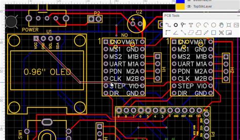
Modern PCB design software, such as Altium Designer, Eagle, and KiCad, offer powerful visualization capabilities. These tools enable designers to create schematic diagrams, assign footprints to components, and generate 3D models of the PCB. By visualizing the design in a realistic manner, designers can identify potential issues early on and make necessary adjustments before moving to the next stage.
Benefits of 3D PCB Visualization
One of the key advantages of PCB visualization is the ability to generate 3D models of the board. 3D visualization provides a more accurate representation of the physical layout, allowing designers to:
- Check for component clearances and potential collisions
- Verify the placement of connectors and other mechanical elements
- Ensure proper heat dissipation and airflow
- Assess the overall aesthetics and ergonomics of the PCB
By catching design flaws early in the process, 3D PCB visualization can save significant time and resources in the long run.

PCB Visualization in the Manufacturing Process
DFM Analysis and Pre-Production Checks
Once the PCB design is finalized, it moves into the manufacturing phase. PCB visualization continues to play a crucial role in this stage, particularly in Design for Manufacturability (DFM) analysis and pre-production checks.
DFM analysis involves reviewing the PCB design to ensure that it can be efficiently manufactured. Visualization tools can help identify potential manufacturing issues, such as:
- Insufficient clearances between components and traces
- Incorrect hole sizes or pad dimensions
- Violations of manufacturing tolerances
- Inconsistencies in the solder mask or silkscreen layers
By addressing these issues before production begins, manufacturers can avoid costly delays and rework.
Virtual Prototyping and Assembly Planning
PCB visualization also enables virtual prototyping and assembly planning. By creating a digital twin of the PCB, manufacturers can simulate the assembly process and optimize their production line. This includes:
- Determining the optimal placement sequence for components
- Identifying potential bottlenecks or challenges in the assembly process
- Verifying the compatibility of the PCB with automated assembly equipment
- Estimating production time and costs
Virtual prototyping allows manufacturers to fine-tune their processes and ensure a smooth transition from design to production.

Collaborating with Stakeholders using PCB Visualization
Effective Communication and Design Reviews
PCB visualization is not only valuable for designers and manufacturers but also for other stakeholders involved in the project. By using clear and accurate visual representations, teams can effectively communicate their ideas and progress to clients, managers, and other departments.
During design reviews, PCB visualization helps to:
- Clearly convey the layout and functionality of the circuit
- Highlight key features and design decisions
- Identify potential issues or areas for improvement
- Facilitate discussions and gather feedback from stakeholders
By fostering effective communication, PCB visualization can help to align everyone’s expectations and ensure that the project stays on track.
Generating Marketing Materials and Documentation
PCB visualization also plays a role in creating marketing materials and technical documentation. High-quality 3D renders of the PCB can be used in product brochures, websites, and presentations to showcase the design and attract potential customers.
Additionally, visualizations can be used to generate clear and concise assembly instructions, user manuals, and other technical documents. By providing visual aids, companies can improve the usability and maintainability of their products, leading to higher customer satisfaction.

Best Practices for Effective PCB Visualization
To maximize the benefits of PCB visualization, consider the following best practices:
-
Choose the right software: Invest in a reliable and feature-rich PCB design software that offers advanced visualization capabilities. Look for tools that support 3D modeling, DFM analysis, and virtual prototyping.
-
Maintain consistent design standards: Establish and adhere to a set of design guidelines and standards to ensure consistency across projects. This includes using standardized component libraries, naming conventions, and layer stackups.
-
Leverage automation: Utilize automated features in your PCB design software, such as design rule checks (DRC) and automatic routing, to streamline the visualization process and reduce the risk of errors.
-
Collaborate effectively: Use cloud-based collaboration tools to share designs and gather feedback from team members and stakeholders. Ensure that everyone has access to the latest version of the design and can provide input in real-time.
-
Continuously review and refine: Regularly review your PCB visualizations and seek opportunities for improvement. Incorporate feedback from manufacturers, assembly teams, and end-users to optimize your designs and visualization practices.
Frequently Asked Questions (FAQ)
-
What is PCB visualization, and why is it important?
PCB visualization refers to the process of creating visual representations of printed circuit boards, including schematic diagrams, 2D layouts, and 3D models. It is essential for effective communication, collaboration, and error prevention throughout the PCB design and manufacturing process. -
What are the benefits of using 3D PCB visualization?
3D PCB visualization provides a more accurate and realistic representation of the physical layout. It allows designers to check for component clearances, verify the placement of connectors, ensure proper heat dissipation, and assess the overall aesthetics and ergonomics of the PCB. -
How does PCB visualization help in the manufacturing process?
PCB visualization enables manufacturers to conduct DFM analysis, identifying potential manufacturing issues such as insufficient clearances, incorrect hole sizes, or violations of manufacturing tolerances. It also facilitates virtual prototyping and assembly planning, allowing manufacturers to optimize their production processes. -
What role does PCB visualization play in collaborating with stakeholders?
PCB visualization helps to effectively communicate design ideas and progress to clients, managers, and other departments. It facilitates design reviews, allowing teams to highlight key features, identify potential issues, and gather feedback from stakeholders. Visualizations can also be used to generate marketing materials and technical documentation. -
What are some best practices for effective PCB visualization?
To maximize the benefits of PCB visualization, choose the right software with advanced visualization capabilities, maintain consistent design standards, leverage automation features, collaborate effectively using cloud-based tools, and continuously review and refine your visualization practices based on feedback from manufacturers, assembly teams, and end-users.
Conclusion
PCB visualization is a powerful tool that can revolutionize the way companies approach PCB design and manufacturing. By leveraging advanced visualization techniques throughout the entire business process, teams can improve communication, catch errors early, and ultimately deliver high-quality products to market faster.
As the electronics industry continues to evolve, investing in robust PCB visualization practices will become increasingly critical for staying competitive. By adopting the best practices outlined in this article and continuously refining their visualization strategies, companies can unlock new levels of efficiency, collaboration, and innovation in their PCB projects.


Leave a Reply