Introduction to PCBs in Robotics
Printed Circuit Boards (PCBs) are the backbone of modern robotics, providing the necessary electrical connections and control systems that bring robots to life. In this comprehensive article, we will delve into the world of PCBs and their crucial role in the field of robotics. From the basic components and manufacturing processes to advanced applications and future trends, we will explore how PCBs are revolutionizing the way we design and build robots.
What are PCBs?
PCBs are thin, flat boards made of insulating materials such as fiberglass or plastic, with conductive copper traces printed onto their surface. These traces form the electrical connections between various components, such as microcontrollers, sensors, and actuators, allowing them to communicate and function as a cohesive system.
Components of a PCB
A typical PCB consists of several key components:
- Substrate: The insulating base material, usually made of fiberglass or plastic.
- Copper layers: Thin sheets of copper laminated onto the substrate, forming the conductive traces.
- Solder mask: A protective coating that covers the copper traces, preventing short circuits and oxidation.
- Silkscreen: A printed layer that adds labels, logos, and other identifying marks to the PCB.
PCB Manufacturing Process
The manufacturing process for PCBs involves several steps:
- Design: The PCB layout is created using specialized software, defining the placement of components and routing of copper traces.
- Printing: The design is printed onto a photosensitive film or directly onto the copper-clad substrate.
- Etching: The unwanted copper is chemically removed, leaving behind the desired traces.
- Drilling: Holes are drilled into the PCB to accommodate through-hole components and vias.
- Plating: The holes are plated with copper to establish electrical connections between layers.
- Solder mask and silkscreen: The protective solder mask and informative silkscreen layers are applied.
- Assembly: Components are soldered onto the PCB, either by hand or using automated pick-and-place machines.

Types of PCBs in Robotics
Robotics applications utilize various types of PCBs, each with its own unique characteristics and benefits.
Single-layer PCBs
Single-layer PCBs have conductive traces on only one side of the substrate. They are the simplest and most cost-effective option, suitable for basic robot control systems and low-complexity designs.
Double-layer PCBs
Double-layer PCBs have conductive traces on both sides of the substrate, allowing for more complex routing and higher component density. They are commonly used in more advanced robot control systems and power distribution boards.
Multi-layer PCBs
Multi-layer PCBs consist of three or more conductive layers, separated by insulating layers. They offer the highest level of complexity and density, enabling the integration of sophisticated control systems, high-speed communication interfaces, and power management solutions.
Flexible PCBs
Flexible PCBs are made from thin, flexible substrates that can bend and conform to various shapes. They are ideal for applications where space is limited or where the PCB needs to move with the robot’s mechanical components, such as in robotic arms or grippers.

PCB Design Considerations for Robotics
Designing PCBs for robotics applications requires careful consideration of several key factors to ensure optimal performance, reliability, and longevity.
Component Selection
Choosing the right components is crucial for the success of a robotic system. Factors to consider include:
- Power requirements
- Temperature ratings
- Packaging (through-hole, surface-mount, or mixed)
- Availability and cost
Signal Integrity
Maintaining signal integrity is essential for reliable communication between components. Designers must consider factors such as:
- Trace width and spacing
- Impedance matching
- Grounding and shielding
- Crosstalk prevention
Power Management
Efficient power management is critical for ensuring the stable operation of robotic systems. Designers must account for:
- Voltage regulation and distribution
- Current capacity and thermal management
- Battery management and charging circuits
- Power sequencing and monitoring
Electromagnetic Compatibility (EMC)
Robotic systems must be designed to minimize electromagnetic interference (EMI) and ensure compatibility with other electronic devices. Considerations include:
- Proper grounding and shielding
- Filtering and suppression techniques
- Compliance with relevant EMC standards and regulations

Advanced PCB Technologies in Robotics
As the field of robotics continues to evolve, so do the PCB technologies that support it. Some of the most notable advancements include:
High-Density Interconnect (HDI) PCBs
HDI PCBs feature finer trace widths, smaller vias, and higher component density than traditional PCBs. They enable the integration of more sophisticated control systems and sensors in smaller form factors, making them ideal for compact and lightweight robotic applications.
Embedded Components
Embedding components, such as resistors, capacitors, and even active devices, directly into the PCB substrate can save space, reduce assembly costs, and improve reliability. This technology is particularly beneficial for miniaturized robotic systems and wearable robotics.
3D PCBs
3D PCBs are a new class of PCBs that combine traditional 2D circuits with 3D structures, such as cavities, channels, and embedded components. They offer unparalleled design flexibility and enable the creation of highly integrated and compact robotic systems.
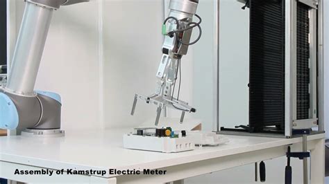
PCB Assembly and Testing for Robotics
Proper assembly and testing are essential for ensuring the reliability and performance of PCBs in robotic systems.
Assembly Techniques
PCB assembly for robotics can be performed using various techniques, including:
- Through-hole assembly: Components with leads are inserted into drilled holes and soldered onto the PCB.
- Surface-mount assembly: Components are placed directly onto the PCB surface and soldered using reflow or wave soldering processes.
- Mixed assembly: A combination of through-hole and surface-mount components are used, catering to the specific requirements of the robotic system.
Testing and Quality Control
Rigorous testing and quality control measures are necessary to guarantee the functionality and durability of PCBs in robotic applications. Common testing methods include:
- Visual inspection: Checking for proper component placement, soldering quality, and any visible defects.
- Automated optical inspection (AOI): Using machine vision systems to detect assembly errors and inconsistencies.
- In-circuit testing (ICT): Verifying the electrical connectivity and functionality of individual components and circuits.
- Functional testing: Evaluating the overall performance of the assembled PCB under real-world operating conditions.
Future Trends in PCBs for Robotics
As the field of robotics continues to advance, PCB technologies must keep pace to support new capabilities and applications.
Miniaturization
The trend towards smaller, more compact robotic systems will drive the development of even more miniaturized PCBs, with finer trace widths, smaller components, and higher-density layouts.
Increased Integration
The integration of more functions and subsystems onto a single PCB will become increasingly common, leading to the development of highly integrated, system-on-a-chip (SoC) solutions for robotics.
Advanced Materials
New substrate materials, such as high-temperature plastics, ceramics, and metal-core PCBs, will enable the creation of PCBs that can withstand harsher operating conditions and support more advanced robotic applications.
Additive Manufacturing
The adoption of additive manufacturing techniques, such as 3D printing, for PCB fabrication will enable faster prototyping, greater design flexibility, and the ability to create complex, non-planar circuit structures.
Conclusion
PCBs play a vital role in the development and advancement of robotics, providing the necessary electrical and control infrastructure that brings robots to life. As the field of robotics continues to evolve, so too will the PCB technologies that support it, driving innovation and enabling new capabilities that were once thought impossible.
By understanding the fundamentals of PCBs, their design considerations, and the latest advancements in the field, robotics engineers and enthusiasts can harness the power of these essential components to create more sophisticated, reliable, and innovative robotic systems.
Frequently Asked Questions (FAQ)
- What are the main advantages of using PCBs in robotics?
PCBs offer several key advantages in robotics, including: - Compact and lightweight design
- Reliable electrical connections
- Simplified assembly and maintenance
Ability to integrate complex control systems and sensors
What are the differences between single-layer, double-layer, and multi-layer PCBs?
- Single-layer PCBs have conductive traces on only one side of the substrate and are suitable for basic robot control systems.
- Double-layer PCBs have conductive traces on both sides of the substrate, allowing for more complex routing and higher component density.
Multi-layer PCBs consist of three or more conductive layers, separated by insulating layers, and offer the highest level of complexity and density.
What factors should be considered when selecting components for a robotic PCB?
When selecting components for a robotic PCB, designers should consider factors such as power requirements, temperature ratings, packaging (through-hole, surface-mount, or mixed), availability, and cost.What is the importance of signal integrity in robotic PCB design?
Maintaining signal integrity is crucial for reliable communication between components in a robotic system. Designers must consider factors such as trace width and spacing, impedance matching, grounding and shielding, and crosstalk prevention to ensure optimal signal integrity.What are some of the future trends in PCBs for robotics?
Some of the key future trends in PCBs for robotics include:- Miniaturization: The development of even more miniaturized PCBs, with finer trace widths, smaller components, and higher-density layouts.
- Increased Integration: The integration of more functions and subsystems onto a single PCB, leading to highly integrated, system-on-a-chip (SoC) solutions.
- Advanced Materials: The use of new substrate materials, such as high-temperature plastics, ceramics, and metal-core PCBs, to support more advanced robotic applications.
- Additive Manufacturing: The adoption of additive manufacturing techniques, such as 3D printing, for faster prototyping and greater design flexibility.
| PCB Type | Layers | Complexity | Cost | Applications |
|---|---|---|---|---|
| Single-layer PCB | 1 | Low | Low | Basic robot control systems |
| Double-layer PCB | 2 | Medium | Medium | Advanced robot control systems |
| Multi-layer PCB | 3+ | High | High | Sophisticated control and power systems |
| Flexible PCB | 1-2 | Medium | Medium | Robotic arms, grippers, wearable robots |


Leave a Reply