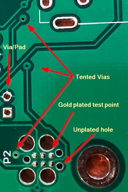
Introduction to Soldermask and Via-holes
Soldermask, also known as solder resist or solder mask, is a thin layer of polymer applied to the copper traces of a printed circuit board (PCB) to protect them from oxidation and prevent solder bridges during the assembly process. It also provides electrical insulation between conductive parts of the PCB. Via-holes, on the other hand, are small holes drilled through the PCB to interconnect different layers of the board electrically.
In the manufacturing of PCBs, various surface finishes can be applied to protect the exposed copper pads and improve solderability. One such surface finish is the chemical Nickel-Gold (ENIG) plating, which consists of a thin layer of gold over a nickel barrier layer. The presence of soldermask on via-holes in the case of ENIG surface finish can have significant implications for the reliability and functionality of the PCB.
The Role of Soldermask in PCB Manufacturing
Soldermask plays a crucial role in PCB manufacturing by:
- Protecting copper traces from oxidation
- Preventing solder bridges during assembly
- Providing electrical insulation between conductive parts
- Improving the aesthetics of the PCB
The soldermask is typically applied using screen printing or photoimaging techniques, and it comes in various colors, with green being the most common.
The Importance of Via-holes in PCBs
Via-holes serve several important functions in PCBs:
- They provide electrical interconnections between different layers of the board
- They help in heat dissipation
- They allow for more compact PCB designs by enabling the routing of traces on multiple layers
Via-holes can be filled or unfilled, depending on the requirements of the PCB design. Filled via-holes offer better mechanical strength and improved thermal conductivity compared to unfilled ones.
Chemical Nickel-Gold (ENIG) Surface Finish
ENIG is a popular surface finish for PCBs due to its excellent solderability, shelf life, and compatibility with various assembly processes. The ENIG plating process involves the following steps:
- Cleaning the PCB surface
- Applying a thin layer of electroless nickel (typically 3-6 µm)
- Applying a thin layer of immersion gold (typically 0.05-0.2 µm) over the nickel layer
The nickel layer acts as a barrier to prevent the diffusion of copper into the gold layer, while the gold layer provides excellent solderability and protection against oxidation.
Advantages of ENIG Surface Finish
- Excellent solderability
- Long shelf life
- Compatibility with various assembly processes
- Good thermal and mechanical stability
- Suitable for fine-pitch components
Disadvantages of ENIG Surface Finish
- Higher cost compared to other surface finishes
- Potential for black pad formation due to excessive phosphorus content in the electroless nickel layer
- Risk of gold embrittlement in thick gold deposits

Soldermask on Via-holes with ENIG Surface Finish
The presence of soldermask on via-holes in the case of ENIG surface finish can have both positive and negative effects on the reliability and functionality of the PCB.
Advantages of Soldermask on Via-holes with ENIG
- Protection of the via-hole from contamination during the assembly process
- Prevention of solder wicking into the via-hole, which can lead to solder defects
- Improved mechanical strength of the via-hole by preventing stress concentration at the edges
- Better electrical insulation between adjacent via-holes
Disadvantages of Soldermask on Via-holes with ENIG
- Difficulty in achieving complete coverage of the via-hole walls with ENIG plating
- Potential for voids or air pockets in the via-hole, leading to reduced thermal and electrical conductivity
- Increased complexity of the manufacturing process, as the soldermask must be selectively removed from the via-holes before ENIG plating
- Risk of soldermask residue on the via-hole walls, which can affect the adhesion of the ENIG plating

Selective Soldermask Removal for Via-holes
To overcome the challenges associated with soldermask on via-holes in the case of ENIG surface finish, selective soldermask removal techniques can be employed. These techniques aim to remove the soldermask from the via-holes while leaving it intact on the rest of the PCB surface.
Laser Ablation
Laser ablation is a popular method for selective soldermask removal. It involves using a high-energy laser beam to vaporize the soldermask material from the via-holes. The advantages of laser ablation include:
- High precision and accuracy
- Minimal damage to the underlying copper
- Fast processing times
- Compatibility with various soldermask materials
However, laser ablation also has some disadvantages, such as:
- High equipment costs
- Potential for thermal damage to the PCB substrate
- Generation of debris that must be cleaned from the via-holes
Plasma Etching
Plasma etching is another method for selective soldermask removal. It involves exposing the PCB to a plasma of reactive gases, which selectively etches away the soldermask material from the via-holes. The advantages of plasma etching include:
- Uniform removal of soldermask
- Minimal damage to the underlying copper
- Compatibility with various soldermask materials
- No generation of debris
However, plasma etching also has some disadvantages, such as:
- Slower processing times compared to laser ablation
- Potential for over-etching, which can damage the PCB substrate
- Higher equipment costs

Best Practices for Soldermask on Via-holes with ENIG
To ensure the reliability and functionality of PCBs with soldermask on via-holes and ENIG surface finish, the following best practices should be followed:
- Use selective soldermask removal techniques to ensure complete coverage of the via-hole walls with ENIG plating
- Optimize the ENIG plating process parameters to minimize the risk of voids or air pockets in the via-holes
- Ensure proper cleaning of the via-holes after soldermask removal to remove any residue that may affect the adhesion of the ENIG plating
- Use filled via-holes wherever possible to improve mechanical strength and thermal conductivity
- Perform thorough quality control inspections to detect any defects or anomalies in the via-holes and ENIG plating
| Parameter | Recommendation |
|---|---|
| Soldermask thickness | 0.5-1.0 mils (12.7-25.4 µm) |
| Via-hole diameter | 0.2-0.5 mm |
| ENIG nickel thickness | 3-6 µm |
| ENIG gold thickness | 0.05-0.2 µm |
| Selective soldermask removal method | Laser ablation or plasma etching |
Frequently Asked Questions (FAQ)
- What is the purpose of soldermask on via-holes?
-
Soldermask on via-holes serves to protect the via-hole from contamination during the assembly process, prevent solder wicking, improve mechanical strength, and provide better electrical insulation between adjacent via-holes.
-
What are the challenges associated with soldermask on via-holes in the case of ENIG surface finish?
-
The main challenges include difficulty in achieving complete coverage of the via-hole walls with ENIG plating, potential for voids or air pockets, increased complexity of the manufacturing process, and risk of soldermask residue affecting the adhesion of the ENIG plating.
-
What are the methods for selective soldermask removal from via-holes?
-
The two primary methods for selective soldermask removal are laser ablation and plasma etching. Laser ablation uses a high-energy laser beam to vaporize the soldermask, while plasma etching employs a plasma of reactive gases to selectively etch away the soldermask.
-
What are the advantages of filled via-holes compared to unfilled ones?
-
Filled via-holes offer better mechanical strength and improved thermal conductivity compared to unfilled via-holes. They also provide a more stable platform for the ENIG plating process.
-
What are the recommended thicknesses for soldermask, ENIG nickel, and ENIG gold layers?
- The recommended soldermask thickness is 0.5-1.0 mils (12.7-25.4 µm), ENIG nickel thickness is 3-6 µm, and ENIG gold thickness is 0.05-0.2 µm.
Conclusion
The presence of soldermask on via-holes in the case of chemical Nickel-Gold (ENIG) surface finish can have significant implications for the reliability and functionality of PCBs. While soldermask on via-holes offers several advantages, such as protection from contamination and improved mechanical strength, it also presents challenges in achieving complete coverage of the via-hole walls with ENIG plating and the potential for voids or air pockets.
To overcome these challenges, selective soldermask removal techniques, such as laser ablation and plasma etching, can be employed. These methods allow for the removal of soldermask from the via-holes while leaving it intact on the rest of the PCB surface, ensuring better coverage of the via-hole walls with ENIG plating.
By following best practices, such as optimizing the ENIG plating process parameters, ensuring proper cleaning of the via-holes after soldermask removal, and using filled via-holes wherever possible, PCB manufacturers can produce high-quality boards with soldermask on via-holes and ENIG surface finish that meet the demanding requirements of modern electronics applications.


Leave a Reply