Introduction to PCB Fabrication
Printed Circuit Board (PCB) fabrication is a complex process that involves multiple steps to create a functional board. One of the critical stages in PCB fabrication is the lay-up and bond process, which is essential for creating multi-layer PCBs. In this article, we will discuss the PCB multi-layer fabrication process, focusing on the lay-up and bond stage.
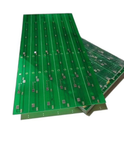
What is a Multi-layer PCB?
A multi-layer PCB is a printed circuit board that consists of multiple layers of conductive copper foil laminated together with insulating materials. The number of layers can vary from four to twelve or more, depending on the complexity of the circuit design. Multi-layer PCBs offer several advantages over single or double-layer boards, including:
- Increased circuit density
- Improved signal integrity
- Better power distribution
- Reduced electromagnetic interference (EMI)
The PCB Fabrication Process
The PCB fabrication process consists of several steps, including:
- Design and layout
- Material selection
- Copper foil lamination
- Drilling
- Plating
- Etching
- Solder mask application
- Silkscreen printing
- Surface finish application
- Electrical testing
Design and Layout
The PCB fabrication process begins with the design and layout of the circuit. The designer creates a schematic diagram of the circuit using specialized software, such as Altium Designer or Eagle. The schematic is then converted into a physical layout, which specifies the location and size of each component, as well as the routing of the copper traces.
Material Selection
The next step in the PCB fabrication process is material selection. The choice of materials depends on the specific requirements of the application, such as the operating temperature, humidity, and mechanical stress. The most common materials used in PCB fabrication are:
- FR-4: A glass-reinforced epoxy laminate that is the most widely used material for PCBs.
- Polyimide: A high-temperature material used in applications that require operation at temperatures up to 260°C.
- PTFE: A low-loss material used in high-frequency applications, such as radar and satellite communication.
Copper Foil Lamination
Once the materials have been selected, the next step is to laminate the copper foil onto the substrate material. The copper foil is typically available in thicknesses ranging from 0.5 oz to 2 oz per square foot. The lamination process involves applying heat and pressure to bond the copper foil to the substrate material.

The Lay-up and Bond Process
The lay-up and bond process is a critical step in the fabrication of multi-layer PCBs. It involves stacking multiple layers of copper foil and insulating material together and bonding them under high pressure and temperature. The process consists of several steps, including:
- Layer preparation
- Lay-up
- Bonding
- Drilling and plating
Layer Preparation
The first step in the lay-up and bond process is to prepare the individual layers of the PCB. Each layer consists of a sheet of copper foil laminated onto a substrate material, such as FR-4. The copper foil is patterned using a photolithographic process to create the desired circuit pattern.
Lay-up
Once the individual layers have been prepared, they are stacked together in a specific order to form the multi-layer PCB. The stack typically consists of alternating layers of copper foil and prepreg (pre-impregnated) material. The prepreg material is a partially cured epoxy resin that acts as an adhesive between the layers.
The lay-up process is performed in a clean room environment to prevent contamination of the PCB. The layers are carefully aligned using registration holes and pins to ensure proper positioning. The stack is then placed in a vacuum press to remove any air between the layers.
Bonding
After the lay-up process is complete, the stack is placed in a bonding press to cure the prepreg material and bond the layers together. The bonding press applies high pressure and temperature to the stack, typically around 350-400 psi and 180-200°C, for a specific duration, usually 1-2 hours.
During the bonding process, the prepreg material melts and flows between the layers, filling any gaps and creating a strong bond. The copper foil on each layer also bonds to the prepreg material, creating a solid, monolithic structure.
Drilling and Plating
After the bonding process is complete, the multi-layer PCB is drilled to create the necessary holes for components and vias. The holes are then plated with copper to create electrical connections between the layers.
The drilling process is typically performed using a computer-controlled drill machine that can drill multiple holes simultaneously with high accuracy. The minimum hole size that can be drilled depends on the thickness of the PCB and the type of drill bit used, but is typically around 0.2 mm.
After drilling, the holes are plated with copper using an electroless plating process. This involves immersing the PCB in a series of chemical baths that deposit a thin layer of copper onto the walls of the holes. The copper plating provides electrical continuity between the layers and enables the mounting of components.

Challenges in Multi-layer PCB Fabrication
While multi-layer PCBs offer many advantages over single or double-layer boards, they also present several challenges in fabrication, including:
Registration and Alignment
One of the biggest challenges in multi-layer PCB fabrication is ensuring proper registration and alignment of the layers. Misalignment can cause short circuits, open circuits, or other defects that can affect the functionality of the PCB. To minimize misalignment, the layers must be carefully aligned using registration holes and pins, and the lay-up process must be performed in a clean room environment.
Thermal Management
Another challenge in multi-layer PCB fabrication is thermal management. As the number of layers increases, the thickness of the PCB also increases, which can lead to heat buildup during operation. To prevent overheating, the PCB must be designed with adequate thermal management features, such as thermal vias, heatsinks, or fans.
Signal Integrity
Signal integrity is another important consideration in multi-layer PCB fabrication. As the number of layers increases, the signal paths become longer and more complex, which can lead to signal degradation, crosstalk, or other issues. To maintain signal integrity, the PCB must be designed with proper impedance control, shielding, and routing techniques.

Quality Control and Testing
To ensure the quality and reliability of multi-layer PCBs, several tests are performed during and after the fabrication process, including:
Visual Inspection
Visual inspection is performed at various stages of the fabrication process to check for defects such as scratches, dents, or contamination. Automated optical inspection (AOI) systems are often used to perform high-speed, high-resolution inspections of the PCB surface.
Electrical Testing
Electrical testing is performed to verify the functionality and performance of the PCB. This includes continuity testing, insulation resistance testing, and high-potential (hipot) testing. These tests ensure that the PCB meets the specified electrical requirements and is free from short circuits, open circuits, or other defects.
Microsectioning
Microsectioning is a destructive testing method that involves cutting a small section of the PCB and examining it under a microscope. This allows the manufacturer to verify the internal structure of the PCB, including the thickness and uniformity of the copper layers, the quality of the drilling and plating, and the presence of any voids or delamination.
Environmental Testing
Environmental testing is performed to verify the durability and reliability of the PCB under various environmental conditions, such as temperature, humidity, and vibration. These tests ensure that the PCB can withstand the expected operating conditions without failure or degradation.
Conclusion
Multi-layer PCB fabrication is a complex process that requires careful design, material selection, and process control. The lay-up and bond process is a critical step in the fabrication of multi-layer PCBs, involving the stacking and bonding of multiple layers of copper foil and insulating material under high pressure and temperature.
While multi-layer PCBs offer many advantages over single or double-layer boards, they also present several challenges in fabrication, including registration and alignment, thermal management, and signal integrity. To ensure the quality and reliability of multi-layer PCBs, several tests are performed during and after the fabrication process, including visual inspection, electrical testing, microsectioning, and environmental testing.
As the demand for high-density, high-performance electronic devices continues to grow, multi-layer PCBs will play an increasingly important role in the electronics industry. By understanding the principles and challenges of multi-layer PCB fabrication, designers and manufacturers can create high-quality, reliable PCBs that meet the needs of modern electronic applications.
FAQs
-
What is the difference between a multi-layer PCB and a single or double-layer PCB?
A multi-layer PCB consists of three or more layers of copper foil laminated together with insulating material, while a single or double-layer PCB has only one or two layers of copper foil. Multi-layer PCBs offer several advantages over single or double-layer boards, including increased circuit density, improved signal integrity, better power distribution, and reduced EMI. -
What materials are commonly used in multi-layer PCB fabrication?
The most common materials used in multi-layer PCB fabrication are FR-4, polyimide, and PTFE. FR-4 is a glass-reinforced epoxy laminate that is widely used for general-purpose applications. Polyimide is a high-temperature material used in applications that require operation at temperatures up to 260°C. PTFE is a low-loss material used in high-frequency applications, such as radar and satellite communication. -
What is the purpose of the prepreg material in the lay-up and bond process?
The prepreg material is a partially cured epoxy resin that acts as an adhesive between the layers of the multi-layer PCB. During the bonding process, the prepreg material melts and flows between the layers, filling any gaps and creating a strong bond between the layers. -
What is the minimum hole size that can be drilled in a multi-layer PCB?
The minimum hole size that can be drilled in a multi-layer PCB depends on the thickness of the PCB and the type of drill bit used, but is typically around 0.2 mm. -
What tests are performed to ensure the quality and reliability of multi-layer PCBs?
Several tests are performed during and after the fabrication process to ensure the quality and reliability of multi-layer PCBs, including visual inspection, electrical testing, microsectioning, and environmental testing. These tests verify the functionality, performance, and durability of the PCB under various operating conditions.
| PCB Type | Advantages | Disadvantages |
|---|---|---|
| Single-layer | Low cost, simple design | Limited circuit density, poor signal integrity |
| Double-layer | Moderate cost, improved signal integrity | Limited circuit density, limited power distribution |
| Multi-layer | High circuit density, excellent signal integrity, good power distribution, reduced EMI | High cost, complex fabrication process, thermal management challenges |


Leave a Reply