What is a PCB?
A Printed Circuit Board (PCB) is a fundamental component in modern electronic devices. It is a flat board made of insulating material, typically fiberglass or composite epoxy, with conductive pathways etched or printed onto its surface. These pathways, also known as traces, connect various electronic components such as resistors, capacitors, integrated circuits, and other elements that make up an electronic circuit.
PCBs serve as the backbone of electronic devices, providing both mechanical support and electrical connectivity for the components. They allow for the miniaturization and standardization of electronic circuits, making them more compact, reliable, and easier to mass-produce.
Types of PCBs
There are several types of PCBs, each designed to meet specific requirements and applications:
-
Single-sided PCBs: These boards have conductive traces on only one side of the insulating substrate. They are the simplest and most cost-effective type of PCB, suitable for basic electronic projects and low-density designs.
-
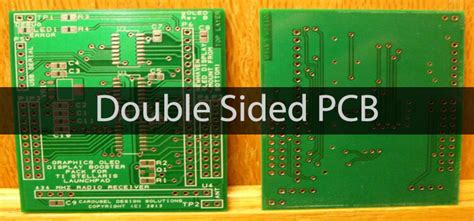
Double-sided PCBs: These boards have conductive traces on both sides of the insulating substrate, allowing for more complex circuits and higher component density. The two sides are connected using through-hole technology or vias.
-
Multi-layer PCBs: These boards consist of three or more conductive layers separated by insulating layers. They offer the highest component density and are used in complex electronic devices such as smartphones, computers, and aerospace systems.
-
Flexible PCBs: These boards are made of flexible insulating materials, allowing them to bend and conform to various shapes. They are commonly used in wearable electronics, medical devices, and applications where space is limited.
-
Rigid-Flex PCBs: These boards combine the features of rigid and flexible PCBs, consisting of both rigid and flexible sections. They are used in applications that require both stability and flexibility, such as automotive electronics and aerospace systems.
PCB Manufacturing Process
The PCB manufacturing process involves several steps, each critical to ensuring the quality and functionality of the final product.
PCB Design
The first step in PCB manufacturing is the design phase. This involves creating a schematic diagram of the electronic circuit and then converting it into a PCB layout using specialized software. The layout determines the placement of components, the routing of traces, and the overall dimensions of the board.
PCB Fabrication
Once the design is finalized, the PCB fabrication process begins. This typically involves the following steps:
-
Substrate preparation: The insulating substrate, usually a copper-clad laminate, is cut to the desired size and shape.
-
Drilling: Holes are drilled into the substrate to accommodate through-hole components and vias.
-
Copper deposition: A thin layer of copper is deposited onto the substrate using electroplating or other methods.
-
Etching: The unwanted copper is removed using a chemical etching process, leaving only the desired conductive traces.
-
Solder mask application: A protective layer, called a solder mask, is applied to the board to insulate the traces and prevent short circuits.
-
Silkscreen printing: Text, logos, and other markings are printed onto the board using silkscreen printing.
-
Surface finish: A surface finish, such as HASL (Hot Air Solder Leveling) or ENIG (Electroless Nickel Immersion Gold), is applied to the exposed copper to prevent oxidation and improve solderability.
PCB Assembly
After the fabrication process, the PCB is ready for assembly. This involves soldering the electronic components onto the board using either through-hole or surface-mount technology (SMT).
-
Through-hole assembly: Components with long leads are inserted into the drilled holes and soldered onto the board manually or using wave soldering machines.
-
Surface-mount assembly: Components with small leads or contact pads are placed directly onto the surface of the board and soldered using reflow soldering machines.
After assembly, the PCB undergoes testing and inspection to ensure proper functionality and adherence to quality standards.

Advantages of PCBs
PCBs offer several advantages over traditional point-to-point wiring and other assembly methods:
-
Compact size: PCBs allow for the miniaturization of electronic devices by accommodating high component density in a small form factor.
-
Reliability: The use of PCBs reduces the risk of loose connections and short circuits, improving the overall reliability of the electronic device.
-
Consistency: PCBs ensure consistent performance across multiple units of the same device, as the manufacturing process is standardized and automated.
-
Cost-effective: Mass production of PCBs is cost-effective, as the manufacturing process can be automated and optimized for high volumes.
-
Design flexibility: PCBs allow for complex circuit designs with multiple layers and high component density, enabling the creation of advanced electronic devices.

Applications of PCBs
PCBs find applications in a wide range of industries and products, including:
-
Consumer electronics: Smartphones, tablets, laptops, televisions, and home appliances.
-
Automotive electronics: Engine control units, infotainment systems, and advanced driver-assistance systems (ADAS).
-
Medical devices: Diagnostic equipment, patient monitoring systems, and implantable devices.
-
Industrial automation: Programmable logic controllers (PLCs), sensors, and control systems.
-
Aerospace and defense: Avionics, radar systems, and satellite communication equipment.
-
IoT devices: Smart home devices, wearables, and remote sensing equipment.
| Industry | Applications |
|---|---|
| Consumer electronics | Smartphones, tablets, laptops, televisions, home appliances |
| Automotive electronics | Engine control units, infotainment systems, ADAS |
| Medical devices | Diagnostic equipment, patient monitoring systems, implantable devices |
| Industrial automation | PLCs, sensors, control systems |
| Aerospace and defense | Avionics, radar systems, satellite communication equipment |
| IoT devices | Smart home devices, wearables, remote sensing equipment |

Future of PCBs
As electronic devices continue to advance and become more complex, the demand for innovative PCB technologies and manufacturing processes will continue to grow. Some of the trends shaping the future of PCBs include:
-
High-speed PCBs: With the increasing demand for faster data transmission and processing, high-speed PCBs that can handle higher frequencies and minimize signal integrity issues will become more prevalent.
-
Miniaturization: The trend towards smaller, more compact electronic devices will drive the development of advanced PCB technologies that enable higher component density and smaller form factors.
-
Flexible and stretchable PCBs: The growth of wearable electronics and the need for conformable devices will lead to the increased adoption of flexible and stretchable PCBs.
-
3D printing: Additive manufacturing techniques, such as 3D printing, may be used to create PCBs with complex geometries and embedded components, offering new design possibilities.
-
Sustainable materials: As environmental concerns grow, there will be a push for the development and use of eco-friendly, recyclable, and biodegradable PCB materials.
Frequently Asked Questions (FAQ)
-
What is the difference between a PCB and a breadboard?
A breadboard is a temporary prototyping tool used to build and test electronic circuits without soldering. PCBs, on the other hand, are permanent, custom-designed boards that provide a reliable and compact solution for electronic circuits. -
Can PCBs be repaired?
Yes, PCBs can be repaired, but the complexity and cost of the repair depend on the extent of the damage and the type of components involved. Simple repairs, such as replacing a single component, can be done by skilled technicians, while more complex repairs may require specialized equipment and expertise. -
How long does it take to manufacture a PCB?
The time required to manufacture a PCB varies depending on the complexity of the design, the size of the order, and the chosen manufacturing process. Simple, single-sided PCBs can be produced in a matter of days, while complex, multi-layer boards may take several weeks. -
What is the minimum feature size of a PCB?
The minimum feature size of a PCB refers to the smallest trace width and spacing that can be reliably produced. This depends on the PCB manufacturing technology and the capabilities of the fabrication facility. Modern PCB manufacturing processes can achieve feature sizes as small as 3-4 mils (0.003-0.004 inches). -
What is the difference between through-hole and surface-mount PCBs?
Through-hole PCBs have components with long leads that are inserted into drilled holes and soldered onto the board. Surface-mount PCBs have components with small leads or contact pads that are placed directly onto the surface of the board and soldered using reflow soldering. Surface-mount technology allows for higher component density and smaller board sizes compared to through-hole technology.
Conclusion
PCBs have revolutionized the electronics industry, enabling the development of compact, reliable, and cost-effective electronic devices. As technology continues to advance, the demand for innovative PCB solutions will only grow, driving the development of new materials, manufacturing processes, and design techniques. By understanding the fundamentals of PCBs, engineers and designers can create cutting-edge electronic products that shape our world and improve our daily lives.


Leave a Reply