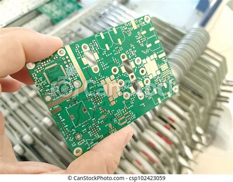
Introduction to RF PCB Assembly
Radio Frequency (RF) PCB assembly is a specialized process that involves the manufacturing and assembly of printed circuit boards designed to operate at high frequencies. These PCBs are crucial components in various applications, such as wireless communication devices, radar systems, and medical equipment. The assembly process for RF PCBs requires a high level of precision and expertise to ensure optimal performance and reliability.
What is RF PCB Assembly?
RF PCB assembly is the process of assembling components onto a printed circuit board that is designed to handle high-frequency signals. This process involves several steps, including:
- PCB fabrication
- Component selection and procurement
- Solder paste application
- Component placement
- Reflow soldering
- Inspection and testing
Each step in the assembly process requires strict adherence to industry standards and best practices to ensure the quality and functionality of the final product.
Importance of RF PCB Assembly
RF PCB assembly plays a vital role in the development and production of electronic devices that rely on high-frequency signals. Some of the key reasons why RF PCB assembly is essential include:
-
Enabling wireless communication: RF PCBs are the backbone of wireless communication devices, such as smartphones, tablets, and laptops.
-
Supporting advanced technologies: RF PCBs are essential for the development and deployment of advanced technologies, such as 5G networks, Internet of Things (IoT) devices, and autonomous vehicles.
-
Ensuring reliability and performance: Proper RF PCB assembly ensures that the final product functions reliably and performs optimally, even under harsh environmental conditions.
RF PCB Design Considerations
Designing an RF PCB requires careful consideration of various factors to ensure optimal performance and reliability. Some of the key design considerations include:
Material Selection
The choice of materials for an RF PCB is crucial, as it directly impacts the board’s performance and reliability. The most common materials used for RF PCBs include:
- FR-4: A cost-effective and widely used material for low-frequency applications.
- Rogers: A high-performance material that offers excellent electrical properties and is suitable for high-frequency applications.
- Teflon: A low-loss material that provides superior dielectric properties and is ideal for ultra-high-frequency applications.
Trace Width and Spacing
The width and spacing of the traces on an RF PCB play a significant role in determining the board’s impedance and signal integrity. The following table provides a general guideline for trace width and spacing based on the desired impedance:
| Impedance (Ω) | Trace Width (mm) | Trace Spacing (mm) |
|---|---|---|
| 50 | 0.25 | 0.25 |
| 75 | 0.20 | 0.30 |
| 100 | 0.15 | 0.35 |
Ground Plane Design
A well-designed ground plane is essential for minimizing noise, reducing electromagnetic interference (EMI), and improving signal integrity in an RF PCB. Some best practices for ground plane design include:
-
Using a solid ground plane: A solid ground plane provides a low-impedance return path for high-frequency signals and helps to minimize noise and EMI.
-
Implementing ground vias: Ground vias help to create a low-impedance connection between the ground plane and the components on the PCB, reducing ground bounce and improving signal integrity.
-
Ensuring proper grounding of components: All components on the RF PCB should be properly grounded to the ground plane to minimize noise and ensure optimal performance.

RF PCB Assembly Process
The RF PCB assembly process involves several critical steps that require precision and expertise. The following sections provide an overview of each step in the process.
PCB Fabrication
PCB fabrication is the first step in the RF PCB assembly process. This step involves creating the bare PCB based on the design specifications provided by the client. The fabrication process typically includes the following sub-steps:
-
Preparing the PCB layout: The PCB layout is created using specialized software, such as Altium Designer or Eagle, based on the schematic and design requirements.
-
Generating Gerber files: Gerber files are the industry-standard format for PCB fabrication and contain all the necessary information for manufacturing the board.
-
Manufacturing the PCB: The bare PCB is manufactured using a combination of etching, drilling, and plating processes based on the Gerber files.
Component Selection and Procurement
Once the bare PCB is fabricated, the next step is to select and procure the components required for the assembly process. This step involves:
-
Identifying the required components: The components required for the RF PCB are identified based on the schematic and bill of materials (BOM) provided by the client.
-
Sourcing the components: The components are sourced from reliable suppliers who can provide high-quality parts that meet the required specifications.
-
Inspecting the components: Upon receipt, the components are inspected to ensure they meet the required quality standards and are free from defects.
Solder Paste Application
Solder paste is a mixture of tiny solder particles suspended in a flux medium. The solder paste is applied to the PCB using a stencil printing process, which involves:
-
Aligning the stencil: The stencil, which has openings that correspond to the pads on the PCB, is aligned with the board using fiducial marks.
-
Applying the solder paste: The solder paste is applied to the stencil using a squeegee, which forces the paste through the openings and onto the pads on the PCB.
-
Inspecting the solder paste: After the solder paste is applied, the PCB is inspected to ensure that the paste is evenly distributed and free from defects.
Component Placement
Once the solder paste is applied, the components are placed onto the PCB using a pick-and-place machine. This process involves:
-
Programming the pick-and-place machine: The pick-and-place machine is programmed with the coordinates of each component on the PCB based on the assembly drawing.
-
Placing the components: The pick-and-place machine uses a vacuum nozzle to pick up each component from the feeder and place it onto the corresponding pads on the PCB.
-
Inspecting the component placement: After the components are placed, the PCB is inspected to ensure that all components are correctly positioned and oriented.
Reflow Soldering
Reflow soldering is the process of melting the solder paste to create a permanent electrical and mechanical connection between the components and the PCB. This process involves:
-
Preheating the PCB: The PCB is preheated to activate the flux in the solder paste and remove any moisture from the board and components.
-
Melting the solder paste: The PCB is then subjected to a controlled temperature profile that melts the solder particles in the paste, allowing them to flow and create a connection between the components and the pads on the PCB.
-
Cooling the PCB: After the solder has melted and formed a connection, the PCB is cooled to allow the solder to solidify and create a permanent bond.
Inspection and Testing
The final step in the RF PCB assembly process is inspection and testing. This step ensures that the assembled PCB meets the required quality standards and functions as intended. Inspection and testing typically involve:
-
Visual inspection: The assembled PCB is visually inspected for any defects, such as bridging, tombstoning, or misaligned components.
-
Automated optical inspection (AOI): AOI machines use high-resolution cameras and advanced software algorithms to detect and classify defects on the PCB.
-
X-ray inspection: X-ray inspection is used to detect defects that are not visible to the naked eye, such as voids in the solder joints or hidden component defects.
-
Functional testing: The assembled PCB is subjected to functional testing to ensure that it performs as intended and meets the required specifications.

Challenges in RF PCB Assembly
RF PCB assembly presents several unique challenges that must be addressed to ensure the quality and reliability of the final product. Some of the key challenges include:
Signal Integrity
Maintaining signal integrity is crucial in RF PCB assembly, as high-frequency signals are sensitive to noise, interference, and distortion. Some strategies for maintaining signal integrity include:
-
Using controlled impedance traces: Controlled impedance traces help to minimize reflections and maintain consistent signal propagation throughout the PCB.
-
Implementing proper grounding and shielding: Proper grounding and shielding techniques help to reduce noise and interference, ensuring that signals remain clean and stable.
-
Minimizing crosstalk: Crosstalk occurs when signals from one trace interfere with signals on adjacent traces. Minimizing crosstalk requires careful design and layout of the PCB, as well as the use of proper isolation techniques.
Thermal Management
RF PCBs often generate significant amounts of heat due to the high-power components used in the design. Effective thermal management is essential to ensure the reliability and longevity of the PCB. Some strategies for thermal management include:
-
Using heat sinks and thermal pads: Heat sinks and thermal pads help to dissipate heat away from critical components, preventing overheating and ensuring optimal performance.
-
Implementing proper airflow: Proper airflow helps to remove heat from the PCB and prevent hot spots from forming, which can lead to component failure.
-
Selecting appropriate components: Selecting components with appropriate power ratings and thermal characteristics helps to minimize heat generation and ensure reliable operation.
Electromagnetic Compatibility (EMC)
EMC is a critical concern in RF PCB assembly, as high-frequency signals can generate significant amounts of electromagnetic interference (EMI). Ensuring EMC requires careful design and testing to minimize EMI and ensure that the PCB complies with relevant industry standards. Some strategies for ensuring EMC include:
-
Implementing proper shielding: Proper shielding helps to contain EMI within the PCB and prevent it from interfering with other electronic devices.
-
Using EMI filters: EMI filters help to suppress high-frequency noise and prevent it from propagating throughout the PCB and beyond.
-
Conducting EMC testing: EMC testing helps to identify potential EMC issues and ensure that the PCB complies with relevant industry standards, such as FCC Part 15 or EN 55022.

Best Practices for RF PCB Assembly
To ensure the quality and reliability of RF PCBs, it is essential to follow best practices throughout the assembly process. Some of the key best practices include:
Supplier Selection
Selecting reliable and experienced suppliers is crucial for ensuring the quality and consistency of the components used in RF PCB assembly. When selecting suppliers, consider factors such as:
-
Quality management systems: Look for suppliers with robust quality management systems, such as ISO 9001 or AS9100, to ensure that they consistently deliver high-quality components.
-
Technical expertise: Choose suppliers with demonstrated technical expertise in RF components and technologies to ensure that they can provide accurate and reliable technical support.
-
Lead times and pricing: Consider the lead times and pricing offered by suppliers to ensure that they align with your project requirements and budget.
Process Control
Implementing strict process controls throughout the RF PCB assembly process helps to ensure consistency, quality, and reliability. Some key process control strategies include:
-
Documenting processes: Clearly document all processes and procedures involved in RF PCB assembly to ensure that they are followed consistently and accurately.
-
Implementing statistical process control (SPC): Use SPC techniques to monitor and control key process parameters, such as solder paste thickness or component placement accuracy, to ensure that they remain within acceptable limits.
-
Conducting regular audits: Conduct regular audits of the assembly process to identify potential issues and opportunities for improvement.
Training and Certification
Investing in training and certification for personnel involved in RF PCB assembly helps to ensure that they have the necessary skills and knowledge to perform their roles effectively. Some key training and certification considerations include:
-
IPC certification: Encourage personnel to obtain relevant IPC certifications, such as IPC-A-610 for acceptability of electronic assemblies or IPC J-STD-001 for soldering.
-
In-house training: Provide in-house training on company-specific processes, procedures, and quality standards to ensure that all personnel are aligned and working towards common goals.
-
Continuous improvement: Foster a culture of continuous improvement by encouraging personnel to identify and share opportunities for enhancing the RF PCB assembly process.
Conclusion
RF PCB assembly is a complex and demanding process that requires a high level of precision, expertise, and attention to detail. By understanding the key design considerations, assembly processes, and best practices involved in RF PCB assembly, engineers and manufacturers can ensure the quality, reliability, and performance of their products.
As the demand for high-frequency electronic devices continues to grow, the importance of RF PCB assembly will only continue to increase. By staying up-to-date with the latest technologies, techniques, and best practices, companies can position themselves to meet this demand and deliver innovative, high-quality products to their customers.
Frequently Asked Questions (FAQ)
-
What is the difference between RF PCB assembly and regular PCB assembly?
RF PCB assembly involves the manufacturing and assembly of PCBs designed to operate at high frequencies, typically above 100 MHz. These PCBs require specialized design considerations, materials, and assembly techniques to ensure optimal performance and reliability. Regular PCB assembly, on the other hand, involves the manufacturing and assembly of PCBs designed for lower-frequency applications. -
What are some common materials used in RF PCB fabrication?
Some common materials used in RF PCB fabrication include FR-4, Rogers, and Teflon. FR-4 is a cost-effective and widely used material for low-frequency applications, while Rogers and Teflon are high-performance materials that offer superior electrical properties and are suitable for high-frequency applications. -
Why is signal integrity important in RF PCB assembly?
Signal integrity is crucial in RF PCB assembly because high-frequency signals are sensitive to noise, interference, and distortion. Maintaining signal integrity helps to ensure that signals remain clean, stable, and free from errors, which is essential for the proper functioning of RF devices. -
What is the purpose of a ground plane in an RF PCB?
A well-designed ground plane in an RF PCB serves several purposes, including minimizing noise, reducing electromagnetic interference (EMI), and improving signal integrity. A solid ground plane provides a low-impedance return path for high-frequency signals and helps to minimize ground bounce and other signal integrity issues. -
What are some strategies for ensuring electromagnetic compatibility (EMC) in RF PCB assembly?
Some strategies for ensuring EMC in RF PCB assembly include implementing proper shielding to contain EMI within the PCB, using EMI filters to suppress high-frequency noise, and conducting thorough EMC testing to identify potential issues and ensure compliance with relevant industry standards.


Leave a Reply