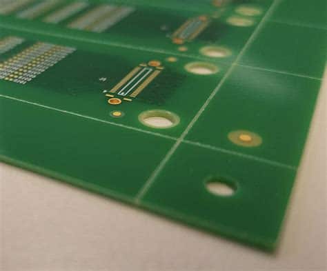
Introduction to PCB Panels
A PCB panel, also known as a PCB array or PCB matrix, is a manufacturing technique used to produce multiple printed circuit boards (PCBs) simultaneously on a single large board. This method is commonly employed to reduce manufacturing costs, improve efficiency, and streamline the assembly process. In this comprehensive guide, we will delve into the various aspects of PCB panels, including their benefits, design considerations, and best practices for optimizing your PCB panel layout.
Benefits of Using PCB Panels
- Cost reduction: Producing multiple PCBs on a single panel reduces the overall manufacturing cost per unit.
- Increased efficiency: Panel-based production allows for faster assembly and processing times.
- Consistent quality: Manufacturing PCBs in a panel ensures consistent quality across all boards in the batch.
- Simplified handling: Panels are easier to handle and transport compared to individual PCBs.
PCB Panel Design Considerations
When designing a PCB panel, several key factors must be taken into account to ensure optimal results. These considerations include panel size, board spacing, tooling holes, fiducial markers, and panel material selection.
Panel Size and Board Spacing
The size of your PCB panel will depend on the dimensions of your individual PCBs and the number of boards you wish to include in a single panel. It is essential to maintain adequate spacing between the boards to ensure proper separation during the depaneling process. The minimum recommended spacing between boards is typically 2-3mm, but this may vary depending on the depaneling method used.
| Depaneling Method | Minimum Board Spacing |
|---|---|
| V-Scoring | 2mm |
| Tab Routing | 2.5mm |
| Perforated Tabs | 3mm |
Tooling Holes and Fiducial Markers
Tooling holes and fiducial markers are critical components of a well-designed PCB panel. Tooling holes are used to secure the panel during the manufacturing process, ensuring accurate alignment and registration. Fiducial markers, on the other hand, serve as reference points for automated assembly equipment, enabling precise component placement.
When incorporating tooling holes and fiducial markers into your PCB panel design, consider the following guidelines:
- Place tooling holes in the corners of the panel, ensuring they do not interfere with the individual PCBs.
- Use a minimum of three fiducial markers per panel, positioned in a triangular pattern for optimal accuracy.
- Ensure that fiducial markers are located away from the edges of the panel and individual PCBs to avoid confusion during the assembly process.
Panel Material Selection
The choice of panel material is crucial for maintaining the structural integrity of your PCBs during the manufacturing and depaneling processes. The most common panel materials include:
- FR-4: A popular choice for its excellent electrical and mechanical properties, as well as its cost-effectiveness.
- Aluminum: Used in applications requiring high thermal conductivity or rigidity.
- Polyimide: Suitable for flexible PCBs and high-temperature applications.
When selecting a panel material, consider the following factors:
- Electrical requirements: Ensure that the material’s dielectric constant and loss tangent are suitable for your application.
- Mechanical properties: Choose a material with adequate strength and rigidity to withstand the manufacturing and depaneling processes.
- Thermal characteristics: Consider the material’s thermal conductivity and expansion coefficients, especially for applications with strict temperature requirements.

Optimizing Your PCB Panel Layout
To maximize the efficiency and cost-effectiveness of your PCB panel design, follow these best practices:
- Minimize waste: Arrange your PCBs on the panel in a way that minimizes unused space and material waste.
- Optimize panel utilization: Maximize the number of PCBs per panel while maintaining adequate spacing and structural integrity.
- Standardize panel sizes: Use standardized panel sizes whenever possible to reduce setup times and costs.
- Incorporate depaneling methods: Select a suitable depaneling method (e.g., V-scoring, tab routing, or perforated tabs) and design your panel accordingly.
- Conduct design reviews: Regularly review your PCB panel designs to identify opportunities for improvement and optimization.

Frequently Asked Questions (FAQ)
- What is the minimum recommended spacing between PCBs on a panel?
-
The minimum recommended spacing between PCBs on a panel is typically 2-3mm, depending on the depaneling method used. V-scoring requires a minimum of 2mm, tab routing requires 2.5mm, and perforated tabs require 3mm.
-
How many fiducial markers should be included on a PCB panel?
-
It is recommended to use a minimum of three fiducial markers per panel, positioned in a triangular pattern for optimal accuracy. This ensures that automated assembly equipment can accurately locate and place components on the individual PCBs.
-
What factors should be considered when selecting a panel material?
-
When selecting a panel material, consider the electrical requirements (dielectric constant and loss tangent), mechanical properties (strength and rigidity), and thermal characteristics (conductivity and expansion coefficients) of the material. Choose a material that is suitable for your specific application and can withstand the manufacturing and depaneling processes.
-
How can I optimize my PCB panel layout for cost-effectiveness?
-
To optimize your PCB panel layout for cost-effectiveness, minimize waste by arranging your PCBs efficiently on the panel, maximize panel utilization by including as many PCBs as possible while maintaining adequate spacing, standardize panel sizes to reduce setup times and costs, and incorporate suitable depaneling methods into your design.
-
Why are design reviews important for PCB panel layouts?
- Conducting regular design reviews is essential for identifying opportunities for improvement and optimization in your PCB panel layouts. By reviewing your designs, you can ensure that your panels are efficiently utilizing material, maintaining structural integrity, and adhering to best practices for manufacturing and assembly. This process can help you reduce costs, improve quality, and streamline your production process.

Conclusion
Designing PCB panels requires careful consideration of various factors, including panel size, board spacing, tooling holes, fiducial markers, and material selection. By adhering to best practices and optimizing your PCB panel layout, you can reduce manufacturing costs, improve efficiency, and ensure consistent quality across your PCBs. Regular design reviews and collaboration with your manufacturing partners can further streamline your production process and help you achieve optimal results.
By following the guidelines outlined in this article and staying up-to-date with industry trends and advancements, you can effectively incorporate PCB panels into your manufacturing strategy and reap the benefits of this powerful production technique.


Leave a Reply