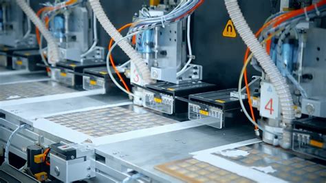
Introduction to PCB machining
Printed Circuit Board (PCB) machining is an essential process in the manufacturing of electronic devices. It involves the creation of holes, slots, and other features on the PCB to accommodate various components and connectors. PCB machining is a complex process that requires precise and accurate methods to ensure the functionality and reliability of the final product.
In this article, we will discuss the different types of PCB machining processes, including slots, milling, contour, and rout-outs. We will also discuss the importance of indicating these features in your PCB design and how to do it effectively.
Types of PCB Machining
Slots
Slots are elongated holes or openings in a PCB that are used to accommodate connectors or other components. They are typically used when a component needs to be inserted into the PCB at an angle or when a connector needs to be mounted on the edge of the board.
Slots can be created using various methods, including:
- Routing: A high-speed rotating tool is used to remove material from the PCB to create the slot.
- Punching: A die is used to punch out the slot shape from the PCB material.
- Laser cutting: A laser is used to cut the slot shape into the PCB material.
When indicating slots in your PCB design, it is important to specify the following:
- Slot dimensions (length, width, and depth)
- Slot location (x and y coordinates)
- Slot orientation (horizontal or vertical)
- Slot tolerances (acceptable variations in dimensions)
Here is an example of how to indicate a slot in your PCB design:
| Feature | Dimension | Location | Orientation | Tolerance |
|---|---|---|---|---|
| Slot | 10mm x 2mm x 1.5mm | (25mm, 50mm) | Horizontal | ±0.1mm |
Milling
Milling is a PCB machining process that involves the use of a rotating cutting tool to remove material from the surface of the PCB. Milling is typically used to create features such as pockets, stepped holes, and cavities on the PCB surface.
Milling can be performed using various methods, including:
- Conventional milling: A rotating cutting tool is used to remove material from the PCB surface in a series of passes.
- Climb milling: The cutting tool moves in the same direction as the rotation of the tool, resulting in a smoother finish and less burring.
- Plunge milling: The cutting tool is plunged vertically into the PCB material to create a hole or cavity.
When indicating milling features in your PCB design, it is important to specify the following:
- Milling dimensions (length, width, and depth)
- Milling location (x and y coordinates)
- Milling tolerances (acceptable variations in dimensions)
- Milling finish (surface roughness)
Here is an example of how to indicate a milled pocket in your PCB design:
| Feature | Dimension | Location | Tolerance | Finish |
|---|---|---|---|---|
| 20mm x 15mm x 1mm | (40mm, 60mm) | ±0.05mm | Ra 0.8μm |
Contour Routing
Contour routing is a PCB machining process that involves the use of a rotating cutting tool to remove material from the edges of the PCB to create a specific shape or profile. Contour routing is typically used to create complex shapes or cutouts on the PCB, such as rounded corners or irregular shapes.
When indicating contour routing features in your PCB design, it is important to specify the following:
- Contour shape and dimensions
- Contour location (x and y coordinates)
- Contour tolerances (acceptable variations in dimensions)
- Contour finish (surface roughness)
Here is an example of how to indicate a contour routed feature in your PCB design:
| Feature | Shape | Dimension | Location | Tolerance | Finish |
|---|---|---|---|---|---|
| Cutout | Circular | Ø10mm | (30mm, 45mm) | ±0.1mm | Ra 1.6μm |
Rout-outs
Rout-outs are a type of PCB machining process that involves the removal of large areas of material from the PCB to create openings or cavities. Rout-outs are typically used to create large openings in the PCB for mounting components or to create cavities for embedding components within the board.
When indicating rout-out features in your PCB design, it is important to specify the following:
- Rout-out dimensions (length, width, and depth)
- Rout-out location (x and y coordinates)
- Rout-out tolerances (acceptable variations in dimensions)
- Rout-out finish (surface roughness)
Here is an example of how to indicate a rout-out feature in your PCB design:
| Feature | Dimension | Location | Tolerance | Finish |
|---|---|---|---|---|
| Rout-out | 50mm x 30mm x 2mm | (60mm, 80mm) | ±0.2mm | Ra 3.2μm |

Importance of Indicating Machining Features in PCB Design
Indicating machining features in your PCB design is crucial for several reasons:
-
Manufacturing accuracy: By clearly specifying the dimensions, locations, and tolerances of machining features, you can ensure that the PCB manufacturer can produce the board accurately and consistently.
-
Design verification: Indicating machining features in your PCB design allows you to verify that the board will meet your requirements and function as intended.
-
Cost reduction: By providing clear and accurate information about machining features, you can help reduce the risk of errors and rework during manufacturing, which can save time and money.
-
Communication: Indicating machining features in your PCB design helps communicate your requirements clearly to the PCB manufacturer and other stakeholders involved in the project.

Best Practices for Indicating Machining Features in PCB Design
To ensure that your PCB design is accurate and manufacturable, follow these best practices when indicating machining features:
-
Use clear and concise language: Use clear and concise language when specifying machining features to avoid confusion or misinterpretation.
-
Provide detailed dimensions: Provide detailed dimensions for each machining feature, including length, width, depth, and location.
-
Specify tolerances: Specify acceptable tolerances for each machining feature to ensure that the PCB manufacturer can produce the board accurately and consistently.
-
Use standard formats: Use standard formats for indicating machining features, such as tables or drawings, to ensure that the information is easy to understand and interpret.
-
Communicate with the PCB manufacturer: Communicate with the PCB manufacturer throughout the design process to ensure that your requirements are understood and can be met.

Conclusion
PCB machining is a critical process in the manufacturing of electronic devices, and indicating machining features in your PCB design is essential for ensuring the accuracy, functionality, and reliability of the final product. By understanding the different types of machining processes and following best practices for indicating machining features, you can help ensure that your PCB design is manufacturable and meets your requirements.
Frequently Asked Questions (FAQ)
-
What is PCB machining?
PCB machining is the process of creating holes, slots, and other features on a printed circuit board (PCB) to accommodate various components and connectors. -
What are the different types of PCB machining processes?
The different types of PCB machining processes include slots, milling, contour routing, and rout-outs. -
Why is it important to indicate machining features in PCB design?
Indicating machining features in PCB design is important for ensuring manufacturing accuracy, design verification, cost reduction, and clear communication with the PCB manufacturer. -
What information should be included when indicating machining features in PCB design?
When indicating machining features in PCB design, it is important to specify the dimensions, location, orientation, tolerances, and finish of each feature. -
What are some best practices for indicating machining features in PCB design?
Some best practices for indicating machining features in PCB design include using clear and concise language, providing detailed dimensions, specifying tolerances, using standard formats, and communicating with the PCB manufacturer throughout the design process.


Leave a Reply