What is Panelising PCBs?
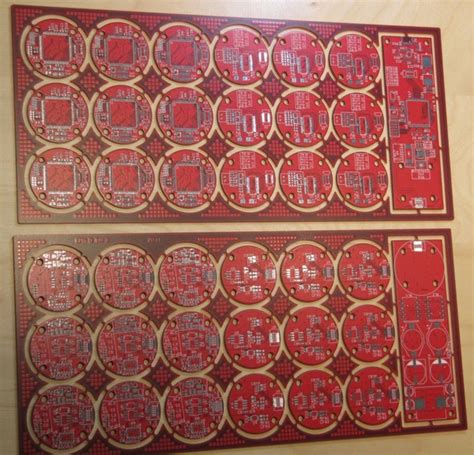
Panelising PCBs refers to the process of combining multiple individual printed circuit boards (PCBs) into a single larger panel. This is done to allow for more efficient and cost-effective manufacturing, as it enables the production of multiple PCBs in a single fabrication run.
When you have a small PCB design, like for a compact electronic device, panelising allows you to produce higher quantities at a lower cost per unit. Instead of manufacturing each tiny PCB individually, which would be time-consuming and expensive, you can group many copies of the PCB design into a panel that fits the standard manufacturing panel sizes used by PCB fabrication houses.
Benefits of Panelising PCBs
Panelising PCBs offers several key benefits:
-
Reduced manufacturing costs: Producing multiple PCBs as a panel is more economical than fabricating them individually since it minimizes material waste and leverages the fixed costs of the manufacturing process across a greater number of units.
-
Faster production times: Panelising streamlines the PCB fabrication process, allowing for quicker turnaround times when you need larger quantities of your small PCB design.
-
Easier handling: Small individual PCBs can be difficult to handle and transport without damage. When combined into a larger panel, they are more robust and easier to work with during the assembly and testing stages of production.
-
Compatibility with assembly equipment: Many automated assembly lines and pick-and-place machines are designed to accommodate standard panel sizes. By panelising your PCBs, you ensure compatibility with this equipment, enabling a smoother assembly process.
Designing Your PCB for Panelisation
To successfully panelise your small PCBs, you need to consider several factors during the PCB design phase:
Board Dimensions and Spacing
When laying out your individual PCB design, keep in mind the dimensions of the standard panel sizes used by your chosen PCB manufacturer. You’ll need to ensure that your PCB can be repeated multiple times within the panel with adequate spacing between each copy.
Typical panel sizes include:
| Panel Size (mm) | Panel Size (inches) |
|---|---|
| 100 x 100 | 3.94 x 3.94 |
| 200 x 200 | 7.87 x 7.87 |
| 300 x 300 | 11.81 x 11.81 |
| 457 x 610 | 18 x 24 |
The spacing between individual PCBs on the panel, known as the “rail width” or “web width,” is usually between 3mm and 5mm. This spacing provides room for tooling holes, fiducial markers, and other features used in the manufacturing process.
Fiducial Markers and Tooling Holes
Fiducial markers are small, precise features added to the PCB design to help align and orient the board during the assembly process. When panelising your PCBs, you should include fiducial markers on both the individual PCBs and the larger panel.
Panel fiducials are typically larger than those on the individual PCBs and are placed in the corners of the panel. They assist with aligning the panel on the assembly line and ensuring accurate placement of components.
Tooling holes are another essential feature for panelised PCBs. These are holes drilled in specific locations on the panel, usually along the edges or in the spaces between individual PCBs. They are used to secure the panel during the various stages of fabrication and assembly and to aid in the depanelization process (separating the individual PCBs from the panel).
Breakaway Tabs or Mouse Bites
To facilitate the separation of individual PCBs from the panel after assembly, you need to include breakaway tabs or “mouse bites” in your panel design. These are small, perforated sections that connect each PCB to the panel frame.
Breakaway tabs are typically 1-2mm wide and are spaced evenly along the edges of each PCB. They are designed to be easily snapped off by hand or with simple tools once the assembly is complete.
Alternatively, mouse bites are small, circular cut-outs arranged in a line between each PCB and the panel frame. They serve the same purpose as breakaway tabs but require less force to separate the boards from the panel.

Panelisation Techniques
There are several methods for panelising PCBs, each with its own advantages and considerations:
Tab Routing
Tab routing is one of the most common panelisation techniques. It involves creating a panel with individual PCBs connected by breakaway tabs, as described earlier. The tabs are milled or routed out during the fabrication process, leaving only small connecting points that can be easily snapped off later.
Advantages of tab routing include:
– Simplicity and ease of use
– Minimal material waste
– Compatibility with most PCB designs
However, tab routing may not be suitable for very small or oddly shaped PCBs, as the tabs can take up valuable space on the panel.
V-Scoring
V-scoring is a technique that creates shallow grooves, usually in a V-shape, along the edges of each individual PCB on the panel. These grooves make it easy to separate the PCBs by snapping them apart, without the need for breakaway tabs.
Advantages of V-scoring:
– Clean, precise board edges after separation
– Reduced space requirements compared to tab routing
– Suitable for small, tightly packed PCB layouts
Disadvantages include:
– Higher cost compared to tab routing
– Potential for stress and damage to the PCB during separation
– Limited compatibility with certain PCB designs and materials
Perforated Boards
Perforated panelisation involves drilling small holes along the edges of each individual PCB on the panel. These holes create a perforated line that allows for easy separation of the boards after assembly.
Advantages:
– Simple and economical technique
– Works well for small, densely packed PCB layouts
– Minimal material waste
Disadvantages:
– Potential for rough or uneven board edges after separation
– May not be suitable for certain applications or environments due to the exposed perforations

Assembly Considerations
When panelising your PCBs, it’s crucial to consider the requirements of the assembly process:
Component Placement and Orientation
Ensure that your component placement and orientation are consistent across all the individual PCBs on the panel. This consistency is essential for automated pick-and-place machines and helps minimize the risk of assembly errors.
Panelisation and Depanelization
Work with your PCB assembly partner to determine the best panelisation method for your specific design and requirements. Consider factors such as the size and shape of your PCBs, the desired board edge quality, and the depanelization process that will be used.
In some cases, the assembly provider may handle the depanelization for you, while in others, you may need to separate the boards yourself after receiving the assembled panels.
Testing and Quality Control
Panelised PCBs can streamline the testing and quality control processes, as multiple boards can be tested simultaneously on the panel before depanelization. This can save time and resources compared to testing individual PCBs.
However, ensure that your testing procedures and equipment are compatible with the panelised format and that any necessary test points or access holes are included in the panel design.

Frequently Asked Questions (FAQ)
-
Q: What is the minimum size for a panelised PCB?
A: The minimum size for a panelised PCB depends on the capabilities of your chosen PCB manufacturer and the specifics of your design. Generally, most manufacturers can accommodate individual PCBs as small as 10mm x 10mm on a panel, but it’s best to consult with your provider to determine their specific requirements and limitations. -
Q: How many individual PCBs can fit on a single panel?
A: The number of individual PCBs that can fit on a single panel varies depending on the size of the PCBs, the panel dimensions, and the spacing between boards. A larger panel can accommodate more PCBs, but the exact number will depend on your specific design and layout. Your PCB manufacturer can help you optimize the panel layout to maximize the number of PCBs per panel. -
Q: Can I panelise PCBs with different designs?
A: Yes, it is possible to panelise PCBs with different designs on a single panel, a technique known as “mixed panelisation.” This can be useful when you need smaller quantities of multiple PCB designs and want to minimize fabrication costs. However, mixed panelisation requires careful planning and layout to ensure that all the designs fit properly on the panel and can be efficiently assembled and depanelized. -
Q: What are the cost benefits of panelising PCBs?
A: Panelising PCBs can offer significant cost savings compared to producing individual boards. By fabricating multiple PCBs on a single panel, you can reduce material waste, minimize setup and tooling costs, and leverage economies of scale. The exact cost savings will depend on factors such as the size of your PCBs, the quantity required, and the complexity of your design. -
Q: How do I choose the best panelisation method for my PCBs?
A: Choosing the best panelisation method for your PCBs depends on several factors, including the size and shape of your individual boards, the desired board edge quality, the assembly process requirements, and the depanelization technique. Tab routing is a common and versatile choice, while V-scoring and perforated panelisation offer advantages for specific applications. Consult with your PCB manufacturer and assembly partner to determine the most suitable method for your project.
Conclusion
Panelising small PCBs is a valuable technique for optimizing the fabrication and assembly processes, reducing costs, and improving production efficiency. By designing your PCBs with panelisation in mind and carefully considering factors such as board dimensions, spacing, fiducial markers, and breakaway tabs, you can successfully create panels that streamline your manufacturing workflow.
When selecting a panelisation method, evaluate your specific requirements and consult with your PCB manufacturer and assembly partner to ensure compatibility and optimal results. With proper planning and execution, panelising your small PCBs can help you achieve high-quality, cost-effective production runs that meet your project’s needs.


Leave a Reply