What is Galvanising and Why is it Important for PCBs?
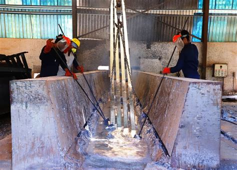
Galvanising is a process of applying a protective zinc coating to steel or iron to prevent rusting. The process involves dipping the metal in a bath of molten zinc, which forms a thin layer of zinc on the surface of the metal. This layer of zinc protects the metal from corrosion by acting as a sacrificial anode, meaning that the zinc will corrode before the metal underneath.
In the context of printed circuit boards (PCBs), galvanising refers to the process of applying a protective coating to the copper traces and pads on the board. This is important because PCBs are often exposed to harsh environments, such as high humidity, temperature fluctuations, and corrosive chemicals. Without proper protection, the copper on the PCB can corrode, leading to electrical shorts, open circuits, and other failures.
Types of Galvanising for PCBs
There are several types of galvanising processes that can be used for PCBs, each with its own advantages and disadvantages. Some of the most common types include:
- Hot Air Solder Leveling (HASL)
- Electroless Nickel Immersion Gold (ENIG)
- Organic Solderability Preservative (OSP)
- Immersion Silver
- Immersion Tin
Hot Air Solder Leveling (HASL)
HASL is one of the most widely used galvanising processes for PCBs. The process involves dipping the PCB in a bath of molten solder, which coats the copper traces and pads with a thin layer of solder. The excess solder is then removed using hot air knives, leaving a smooth, flat surface.
Advantages of HASL include:
- Low cost
- Good solderability
- Excellent shelf life
- Compatible with most soldering processes
Disadvantages of HASL include:
- Uneven surface finish
- Potential for solder bridges
- Not suitable for fine-pitch components
- Contains lead (Pb), which is restricted by RoHS regulations
Electroless Nickel Immersion Gold (ENIG)
ENIG is a two-step process that involves depositing a layer of nickel on the copper traces and pads, followed by a thin layer of gold. The nickel layer provides a barrier against copper diffusion and oxidation, while the gold layer provides excellent solderability and protection against corrosion.
Advantages of ENIG include:
- Flat, even surface finish
- Excellent solderability
- Good shelf life
- RoHS compliant
- Suitable for fine-pitch components
Disadvantages of ENIG include:
- Higher cost than HASL
- Potential for “black pad” defects due to excessive nickel buildup
- Requires strict process control to prevent defects
Organic Solderability Preservative (OSP)
OSP is a chemical coating that is applied to the copper traces and pads on the PCB. The coating forms a thin, organic layer that protects the copper from oxidation and provides good solderability.
Advantages of OSP include:
- Low cost
- Flat, even surface finish
- RoHS compliant
- Suitable for fine-pitch components
Disadvantages of OSP include:
- Limited shelf life (typically 6-12 months)
- Requires careful handling to prevent damage to the coating
- May require additional cleaning steps prior to soldering
Immersion Silver
Immersion silver is a process that involves depositing a thin layer of silver on the copper traces and pads of the PCB. The silver layer provides excellent solderability and protection against oxidation.
Advantages of immersion silver include:
- Flat, even surface finish
- Excellent solderability
- RoHS compliant
- Suitable for fine-pitch components
Disadvantages of immersion silver include:
- Higher cost than OSP
- Limited shelf life (typically 6-12 months)
- Potential for silver migration, which can cause electrical shorts
Immersion Tin
Immersion tin is a process that involves depositing a thin layer of tin on the copper traces and pads of the PCB. The tin layer provides good solderability and protection against oxidation.
Advantages of immersion tin include:
- Low cost
- Flat, even surface finish
- RoHS compliant
- Suitable for fine-pitch components
Disadvantages of immersion tin include:
- Limited shelf life (typically 6-12 months)
- Potential for tin whiskers, which can cause electrical shorts
- May require additional cleaning steps prior to soldering
Factors to Consider When Choosing a Galvanising Process for PCBs
When choosing a galvanising process for PCBs, there are several factors to consider, including:
- Cost
- Shelf life
- Solderability
- Compatibility with components
- Environmental regulations
Cost
The cost of the galvanising process is an important consideration, especially for high-volume production. HASL and OSP are generally the lowest cost options, while ENIG and immersion silver are more expensive.
Shelf Life
The shelf life of the PCB is another important factor to consider. HASL and ENIG have the longest shelf life, typically several years, while OSP and immersion silver have shorter shelf lives, typically 6-12 months.
Solderability
The solderability of the PCB is critical for ensuring reliable electrical connections. HASL, ENIG, and immersion silver provide excellent solderability, while OSP and immersion tin may require additional cleaning steps prior to soldering.
Compatibility with Components
The compatibility of the galvanising process with the components used on the PCB is another important consideration. Fine-pitch components, such as ball grid arrays (BGAs) and quad flat no-leads (QFNs), require a flat, even surface finish, which can be achieved with ENIG, OSP, immersion silver, or immersion tin.
Environmental Regulations
Environmental regulations, such as the Restriction of Hazardous Substances (RoHS) directive, may restrict the use of certain materials, such as lead, in PCBs. HASL contains lead, which is restricted by RoHS, while ENIG, OSP, immersion silver, and immersion tin are RoHS compliant.

The Galvanising Process for PCBs
The galvanising process for PCBs typically involves several steps, including:
- Cleaning
- Microetching
- Activation
- Deposition
- Rinsing and drying
Cleaning
The first step in the galvanising process is to clean the PCB to remove any contaminants, such as dirt, grease, and oxidation. This is typically done using a combination of mechanical and chemical cleaning methods, such as brushing, scrubbing, and dipping in cleaning solutions.
Microetching
After cleaning, the PCB is often subjected to a microetching process, which removes a thin layer of copper from the surface of the traces and pads. This helps to improve the adhesion of the galvanising layer and ensures a uniform surface finish.
Activation
The next step is to activate the surface of the copper to promote the deposition of the galvanising layer. This is typically done using a chemical solution that contains a catalyst, such as palladium or nickel.
Deposition
The actual deposition of the galvanising layer occurs in this step. The PCB is immersed in a bath containing the galvanising solution, which may be a molten metal, such as solder or tin, or a chemical solution, such as electroless nickel or immersion gold.
Rinsing and Drying
After deposition, the PCB is rinsed to remove any excess galvanising solution and then dried to prevent oxidation and contamination.

Troubleshooting Common Issues with Galvanised PCBs
Despite the benefits of galvanising, there are several common issues that can arise with galvanised PCBs, including:
- Solder bridges
- Black pad defects
- Tin whiskers
- Silver migration
Solder Bridges
Solder bridges are a common issue with HASL-coated PCBs, where excess solder connects adjacent pads or traces, causing electrical shorts. This can be prevented by using a solder mask to cover the areas between the pads and traces, or by using a different galvanising process, such as ENIG or OSP.
Black Pad Defects
Black pad defects are a common issue with ENIG-coated PCBs, where the nickel layer becomes excessively thick and brittle, causing the solder joint to fail. This can be prevented by careful process control to ensure that the nickel layer is deposited uniformly and to the correct thickness.
Tin Whiskers
Tin whiskers are a common issue with immersion tin-coated PCBs, where thin, conductive filaments of tin grow from the surface of the PCB, potentially causing electrical shorts. This can be prevented by using a different galvanising process, such as ENIG or OSP, or by using a tin-lead alloy instead of pure tin.
Silver Migration
Silver migration is a common issue with immersion silver-coated PCBs, where silver ions migrate through the PCB substrate, potentially causing electrical shorts. This can be prevented by using a different galvanising process, such as ENIG or OSP, or by using a silver-palladium alloy instead of pure silver.

Frequently Asked Questions (FAQ)
- What is the best galvanising process for PCBs?
There is no one “best” galvanising process for PCBs, as the choice depends on several factors, such as cost, shelf life, solderability, compatibility with components, and environmental regulations. HASL and ENIG are the most commonly used processes, but OSP, immersion silver, and immersion tin may be suitable for certain applications.
- Can galvanised PCBs be reworked?
Yes, galvanised PCBs can be reworked, but the process depends on the type of galvanising used. HASL and ENIG are the easiest to rework, as the solder can be easily removed and replaced. OSP and immersion silver may require additional cleaning steps prior to rework, while immersion tin may be more difficult to rework due to the potential for tin whiskers.
- How long do galvanised PCBs last?
The shelf life of galvanised PCBs depends on the type of galvanising used. HASL and ENIG have the longest shelf life, typically several years, while OSP and immersion silver have shorter shelf lives, typically 6-12 months. However, the actual lifespan of the PCB depends on several factors, such as the operating environment, the quality of the materials and workmanship, and the level of maintenance and care.
- Are galvanised PCBs environmentally friendly?
The environmental friendliness of galvanised PCBs depends on the type of galvanising used. HASL contains lead, which is restricted by RoHS regulations, while ENIG, OSP, immersion silver, and immersion tin are RoHS compliant. However, the production of PCBs involves the use of chemicals and energy, so the overall environmental impact should be considered.
- Can galvanised PCBs be used in high-temperature applications?
Yes, galvanised PCBs can be used in high-temperature applications, but the choice of galvanising process depends on the specific requirements. ENIG and immersion silver are suitable for high-temperature applications up to 150°C, while OSP and immersion tin are suitable for applications up to 125°C. HASL is not recommended for high-temperature applications due to the potential for solder reflow and delamination.
In conclusion, galvanising is an important process for protecting PCBs from corrosion and ensuring reliable electrical connections. There are several types of galvanising processes available, each with its own advantages and disadvantages, and the choice depends on several factors, such as cost, shelf life, solderability, compatibility with components, and environmental regulations. By understanding the galvanising process and the common issues that can arise, PCB designers and manufacturers can ensure the production of high-quality, reliable PCBs that meet the specific requirements of the application.


Leave a Reply