What is PCB Population?
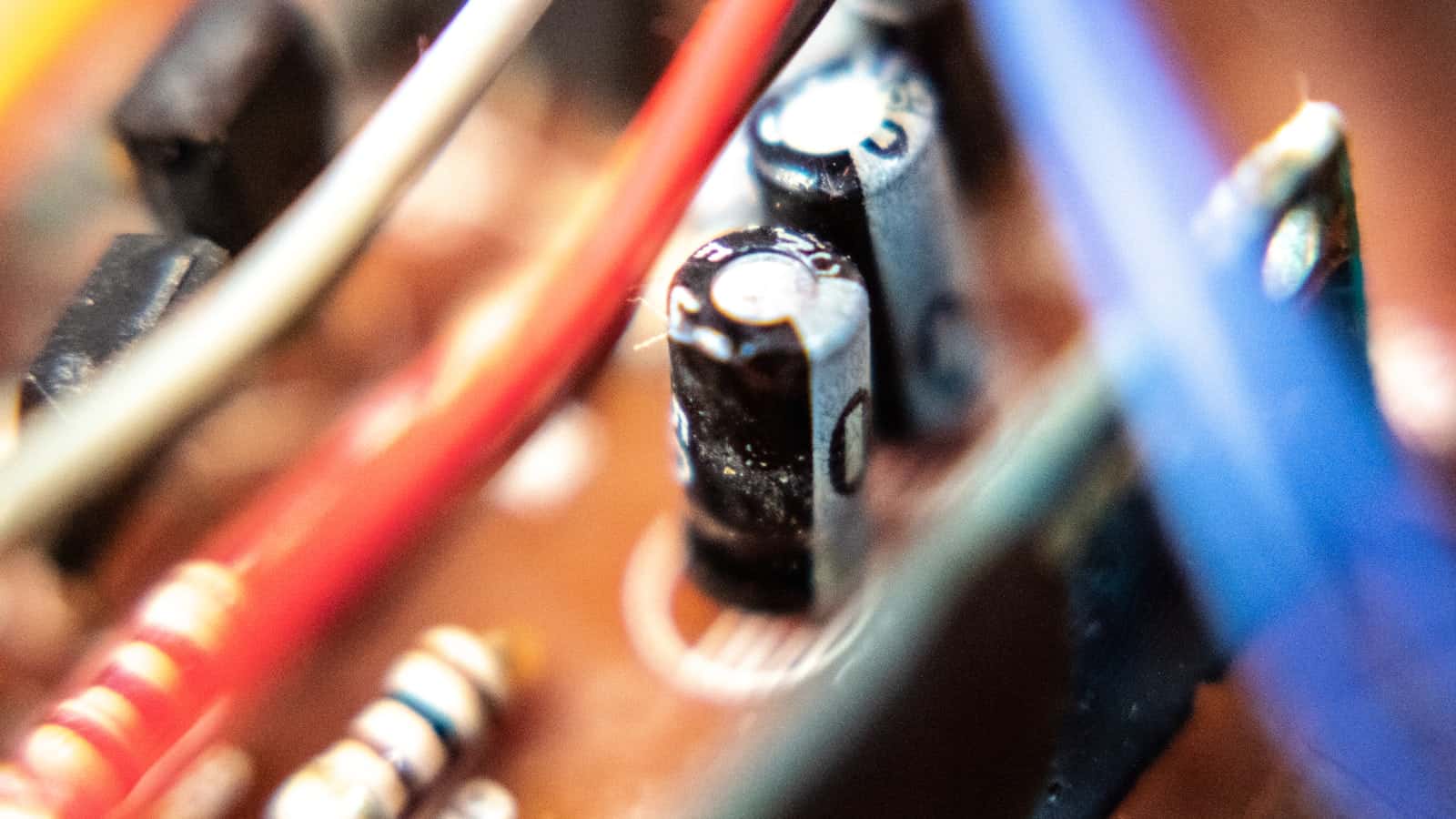
PCB population, also known as PCB assembly or PCBA, is the process of attaching electronic components to a printed circuit board (PCB). This process involves placing and soldering various components, such as resistors, capacitors, integrated circuits (ICs), and connectors, onto the PCB to create a functional electronic device.
The Importance of PCB Population
PCB population is a crucial step in the manufacturing of electronic devices. It directly impacts the functionality, reliability, and quality of the final product. Proper PCB population ensures that:
- Components are placed accurately and securely on the PCB
- Electrical connections are established between components
- The device functions as intended
- The device is reliable and durable
PCB Population Methods
There are two primary methods for populating PCBs: through-hole technology (THT) and surface mount technology (SMT). Each method has its advantages and is suitable for different applications.
Through-Hole Technology (THT)
Through-hole technology involves inserting component leads through drilled holes in the PCB and soldering them to pads on the opposite side. This method is older and less common than SMT but is still used for certain components and applications.
Advantages of THT:
– Stronger mechanical bonds between components and the PCB
– Suitable for larger, heavier components
– Easier to solder manually
Disadvantages of THT:
– Requires drilling holes in the PCB
– Consumes more space on the PCB
– Slower assembly process compared to SMT
Surface Mount Technology (SMT)
Surface mount technology involves placing components directly onto pads on the surface of the PCB and soldering them in place. SMT is the most common method for PCB population due to its numerous advantages.
Advantages of SMT:
– Allows for smaller component sizes and higher component density
– Faster assembly process using automated equipment
– Enables double-sided PCB assembly
– Reduces manufacturing costs
Disadvantages of SMT:
– Requires specialized equipment for assembly
– More sensitive to thermal stress during soldering
– Harder to solder manually
The PCB Population Process
The PCB population process typically involves the following steps:
-
Solder Paste Application: Solder paste, a mixture of tiny solder particles and flux, is applied to the PCB pads using a stencil or screen printing process.
-
Component Placement: Components are placed onto the solder paste-covered pads using automated pick-and-place machines or manual placement for smaller production runs.
-
Reflow Soldering: The PCB with placed components is passed through a reflow oven, which heats the solder paste to its melting point, allowing it to form a strong electrical and mechanical bond between the components and the PCB pads.
-
Inspection and Quality Control: The populated pcb undergoes visual inspection and automated optical inspection (AOI) to identify any defects, such as misaligned components, solder bridges, or insufficient solder joints.
-
Rework and Repair: If defects are found during inspection, the PCB is sent for rework and repair, where the issues are corrected manually or using specialized equipment.
-
Testing: The populated PCB is tested for functionality, performance, and compliance with specifications using various methods, such as in-circuit testing (ICT), boundary scan testing, or functional testing.
-
Conformal Coating and Final Assembly: Depending on the application, the populated PCB may receive a conformal coating to protect it from environmental factors like moisture, dust, or chemicals. Finally, the PCB is integrated into the final product assembly.

Equipment Used in PCB Population
PCB population relies on various types of equipment to ensure accurate, efficient, and reliable assembly. Some of the key equipment used in the process include:
Stencil Printer
A stencil printer is used to apply solder paste to the PCB pads. It consists of a frame that holds a stencil with openings corresponding to the PCB pads, a squeegee to spread the solder paste, and a mechanism to align the PCB with the stencil.
Pick-and-Place Machine
Pick-and-place machines are automated systems that place components onto the PCB with high speed and precision. They use vacuum nozzles or grippers to pick up components from feeders and place them onto the solder paste-covered pads.
| Machine Type | Speed (components per hour) | Placement Accuracy |
|---|---|---|
| High-speed | 50,000 – 200,000 | ±50 μm |
| Mid-range | 10,000 – 50,000 | ±100 μm |
| Entry-level | 1,000 – 10,000 | ±200 μm |
Reflow Oven
A reflow oven is used to melt the solder paste and form a strong bond between the components and the PCB pads. It consists of multiple heating zones that gradually raise the temperature of the PCB to the solder’s melting point and then cool it down in a controlled manner.
Automated Optical Inspection (AOI) System
AOI systems use high-resolution cameras and advanced image processing algorithms to inspect the populated PCB for defects such as misaligned components, solder bridges, or insufficient solder joints. They can quickly identify issues and provide feedback for rework and repair.
Challenges in PCB Population
PCB population can present several challenges that manufacturers must address to ensure the quality and reliability of the final product:
-
Component Miniaturization: As electronic devices become smaller and more complex, component sizes continue to shrink, making it more challenging to place and solder them accurately.
-
High-Density Layouts: PCBs with high component density require precise placement and soldering to avoid defects like solder bridges or shorts.
-
Thermal Management: Certain components, such as power ICs or high-performance processors, generate significant heat that must be dissipated effectively to prevent damage to the PCB or other components.
-
Electrostatic Discharge (ESD) Protection: Many electronic components are sensitive to ESD, which can cause damage during handling and assembly. Proper ESD protection measures must be implemented throughout the PCB population process.
-
Counterfeit Components: Counterfeit or substandard components can compromise the quality and reliability of the populated PCB. Manufacturers must have strict quality control measures in place to prevent the use of counterfeit components.
FAQ
-
Q: What is the difference between PCB population and PCB fabrication?
A: PCB fabrication is the process of creating the bare PCB, which includes designing the circuit, printing the copper traces, and applying the solder mask and silkscreen. PCB population, on the other hand, is the process of attaching components to the fabricated PCB. -
Q: Can PCBs be populated manually?
A: Yes, PCBs can be populated manually, especially for low-volume production or prototyping. However, manual population is slower, less precise, and more prone to human error compared to automated methods like pick-and-place machines. -
Q: What is the purpose of solder paste in PCB population?
A: Solder paste serves two main purposes in PCB population. First, it provides a temporary adhesive to hold the components in place before soldering. Second, it contains the solder that, when melted, forms the electrical and mechanical connection between the component leads and the PCB pads. -
Q: How does the reflow soldering process work?
A: In reflow soldering, the PCB with solder paste and placed components is passed through a reflow oven. The oven gradually heats the PCB, causing the solder paste to melt and form a strong bond between the components and the PCB pads. The PCB is then cooled in a controlled manner to solidify the solder joints. -
Q: What are some common defects that can occur during PCB population?
A: Common defects in PCB population include misaligned components, solder bridges (unintended connections between pads), insufficient or excessive solder, tombstoning (components standing on one end), and damaged components due to improper handling or thermal stress.
Conclusion
PCB population is a critical process in the manufacturing of electronic devices, directly impacting the functionality, reliability, and quality of the final product. Through-hole technology and surface mount technology are the two primary methods used for PCB population, each with its advantages and suitable applications.
The PCB population process involves several steps, including solder paste application, component placement, reflow soldering, inspection, rework, testing, and final assembly. Various equipment, such as stencil printers, pick-and-place machines, reflow ovens, and AOI systems, are used to ensure accurate, efficient, and reliable assembly.
Manufacturers must address challenges like component miniaturization, high-density layouts, thermal management, ESD protection, and counterfeit components to ensure the quality and reliability of the populated PCBs.
As electronic devices continue to evolve and become more complex, advancements in PCB population techniques and equipment will be essential to meet the growing demands for smaller, faster, and more reliable electronic products.


Leave a Reply