Introduction to PCB Circuit Design
Printed Circuit Boards (PCBs) are the backbone of modern electronics. They provide a platform for mounting and interconnecting electronic components to create complex circuits and systems. PCB circuit design involves creating a layout of conductive tracks, pads, and other features on a non-conductive substrate to form the desired electrical connections between components.
Proper PCB circuit design is crucial for the functionality, reliability, and manufacturability of electronic devices. It requires careful consideration of various factors such as component selection, signal integrity, power distribution, thermal management, and manufacturing constraints.
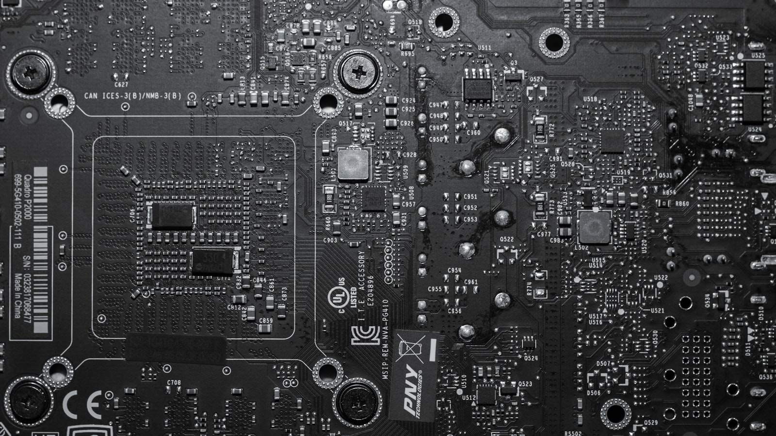
One often overlooked aspect of PCB circuit design is labeling. PCB labeling refers to the practice of adding text, symbols, or other markings on the PCB to provide information about components, connections, and other design elements. In this article, we will explore the importance of PCB labeling and how it contributes to the success of PCB circuit design.
The Role of PCB Labeling in Circuit Design
PCB labeling serves several important functions in circuit design:
-
Component Identification: Labels help identify components on the PCB, making it easier for designers, assemblers, and technicians to locate and work with specific parts.
-
Orientation and Polarity: Labels can indicate the orientation and polarity of components, ensuring correct placement and preventing assembly errors.
-
Signal Tracing: Labels can be used to identify signal traces, making it easier to follow the flow of signals through the circuit during troubleshooting or debugging.
-
Version Control: Labels can include version numbers or other identifiers to track different revisions of the PCB design.
-
Regulatory Compliance: Labels can provide information required by regulatory standards, such as safety warnings, certification marks, or disposal instructions.
By incorporating clear and informative labels into the PCB design, designers can improve the efficiency and accuracy of the manufacturing process, reduce the risk of errors, and facilitate maintenance and repairs.
Types of PCB Labels
There are various types of labels that can be used in PCB circuit design, each serving different purposes:
Text Labels
Text labels are the most common type of PCB label. They consist of alphanumeric characters and can be used to identify components, signal traces, test points, and other features. Text labels are typically created using silk screen printing or direct legend printing techniques.
Graphic Symbols
Graphic symbols are pictorial representations used to convey information about components or functions. Common examples include polarity markers, pin numbering, and logos. Graphic symbols can be more intuitive and easier to recognize than text labels, especially for complex or standardized components.
Fiducial Marks
Fiducial marks are reference points used by automated assembly equipment to align and position the PCB during manufacturing. They are typically small, round, or cross-shaped marks placed at specific locations on the PCB. Fiducial marks ensure precise and consistent placement of components, improving the accuracy and reliability of the assembly process.
Bar Codes and QR Codes
Bar codes and QR codes are machine-readable labels that can store more information than traditional text or graphic labels. They can be used to encode part numbers, serial numbers, or other identifying information. Bar codes and QR codes enable automated tracking and traceability of PCBs throughout the manufacturing and supply chain process.

Design Considerations for PCB Labeling
When incorporating labels into PCB circuit design, designers should consider the following factors:
Readability
Labels should be clearly legible and easy to read. This requires selecting an appropriate font style, size, and color contrast. Labels should also be positioned in a way that minimizes interference with other design elements and ensures visibility during assembly and inspection.
Placement
The placement of labels should be carefully considered to avoid interfering with component mounting, soldering, or other manufacturing processes. Labels should also be located in areas that are accessible for inspection and debugging.
Durability
Labels should be able to withstand the environmental conditions and handling processes involved in PCB manufacturing and use. This may require using inks or materials that are resistant to solvents, heat, or abrasion.
Language and Symbols
Labels should use standardized language and symbols wherever possible to ensure consistency and avoid confusion. Industry-specific standards, such as IPC or ANSI, provide guidelines for labeling conventions.
Size and Spacing
The size and spacing of labels should be appropriate for the available space on the PCB and the intended use of the labels. Overcrowding labels can lead to readability issues and manufacturing challenges.
Benefits of Effective PCB Labeling
Effective PCB labeling offers several benefits for circuit design and manufacturing:
-
Improved Assembly Efficiency: Clear and accurate labels help assemblers quickly identify and place components, reducing the time and effort required for manual assembly processes.
-
Reduced Assembly Errors: Labels that indicate component orientation, polarity, and other critical information can prevent common assembly errors, such as reversed or misaligned components.
-
Enhanced Troubleshooting and Debugging: Well-labeled PCBs are easier to troubleshoot and debug, as technicians can quickly identify components and trace signals through the circuit.
-
Faster Repairs and Maintenance: Labels that identify components and their functions enable technicians to locate and replace faulty parts more efficiently, minimizing downtime and repair costs.
-
Improved Documentation and Communication: Labels provide a visual reference that can be used in documentation, such as assembly instructions, schematics, and bill of materials (BOM). This improves communication between design, manufacturing, and maintenance teams.
Examples of PCB Labeling
To illustrate the use of PCB labeling, let’s consider a few examples:
Example 1: Simple Resistor Label
A basic resistor label might include the component designator (e.g., R1, R2) and the resistance value (e.g., 10K, 4.7K). This information helps assemblers identify and place the correct resistor in the designated location.
| Label | Description |
|---|---|
| R1 | Resistor 1 |
| 10K | 10 kilo-ohm resistance |
Example 2: Integrated Circuit (IC) Label
An IC label typically includes the component designator, the IC type or part number, and a pin 1 indicator. Additional information, such as the manufacturer’s logo or the IC function, may also be included.
| Label | Description |
|---|---|
| U1 | IC designator |
| ATmega328 | IC part number |
| • | Pin 1 indicator |
Example 3: Connector Label
Connector labels often include the connector designator, the connector type, and pin numbers or signal names. This information helps ensure proper wiring and signal connections.
| Label | Description |
|---|---|
| J1 | Connector designator |
| USB | Connector type |
| VCC, D+, D-, GND | Pin signal names |
FAQ
Q: What is the purpose of PCB labeling?
A: PCB labeling is used to provide information about components, connections, and other design elements on a printed circuit board. It helps identify parts, indicate orientation and polarity, trace signals, track versions, and ensure regulatory compliance.
Q: What are the different types of PCB labels?
A: The main types of PCB labels include text labels, graphic symbols, fiducial marks, and bar codes or QR codes. Text labels use alphanumeric characters, graphic symbols are pictorial representations, fiducial marks are reference points for alignment, and bar codes or QR codes store machine-readable information.
Q: What factors should be considered when designing PCB labels?
A: When designing PCB labels, important factors to consider include readability, placement, durability, language and symbols, and size and spacing. Labels should be clear, properly positioned, resistant to environmental conditions, consistent with standards, and appropriately sized.
Q: How does PCB labeling benefit the manufacturing process?
A: PCB labeling improves assembly efficiency by helping assemblers quickly identify and place components. It reduces assembly errors by indicating orientation and polarity. Well-labeled PCBs are easier to troubleshoot, debug, and repair, saving time and costs. Labels also enhance documentation and communication between teams.
Q: Are there any industry standards for PCB labeling?
A: Yes, industry organizations such as IPC (Association Connecting Electronics Industries) and ANSI (American National Standards Institute) provide guidelines and standards for PCB labeling conventions. These standards help ensure consistency and clarity in labeling practices across the electronics industry.
Conclusion
PCB labeling is a crucial aspect of PCB circuit design that should not be overlooked. Labels provide essential information about components, connections, and other design elements, enabling efficient assembly, troubleshooting, and maintenance of electronic devices.
By incorporating clear, durable, and standardized labels into PCB designs, designers can improve the manufacturability, reliability, and serviceability of their products. Effective labeling practices reduce errors, save time and costs, and enhance communication throughout the product lifecycle.
As PCB designs continue to increase in complexity, the importance of accurate and informative labeling will only grow. By understanding the types, design considerations, and benefits of PCB labeling, designers can create PCBs that are not only functionally sound but also user-friendly and maintainable.


Leave a Reply