PCB Assembly Blog
-
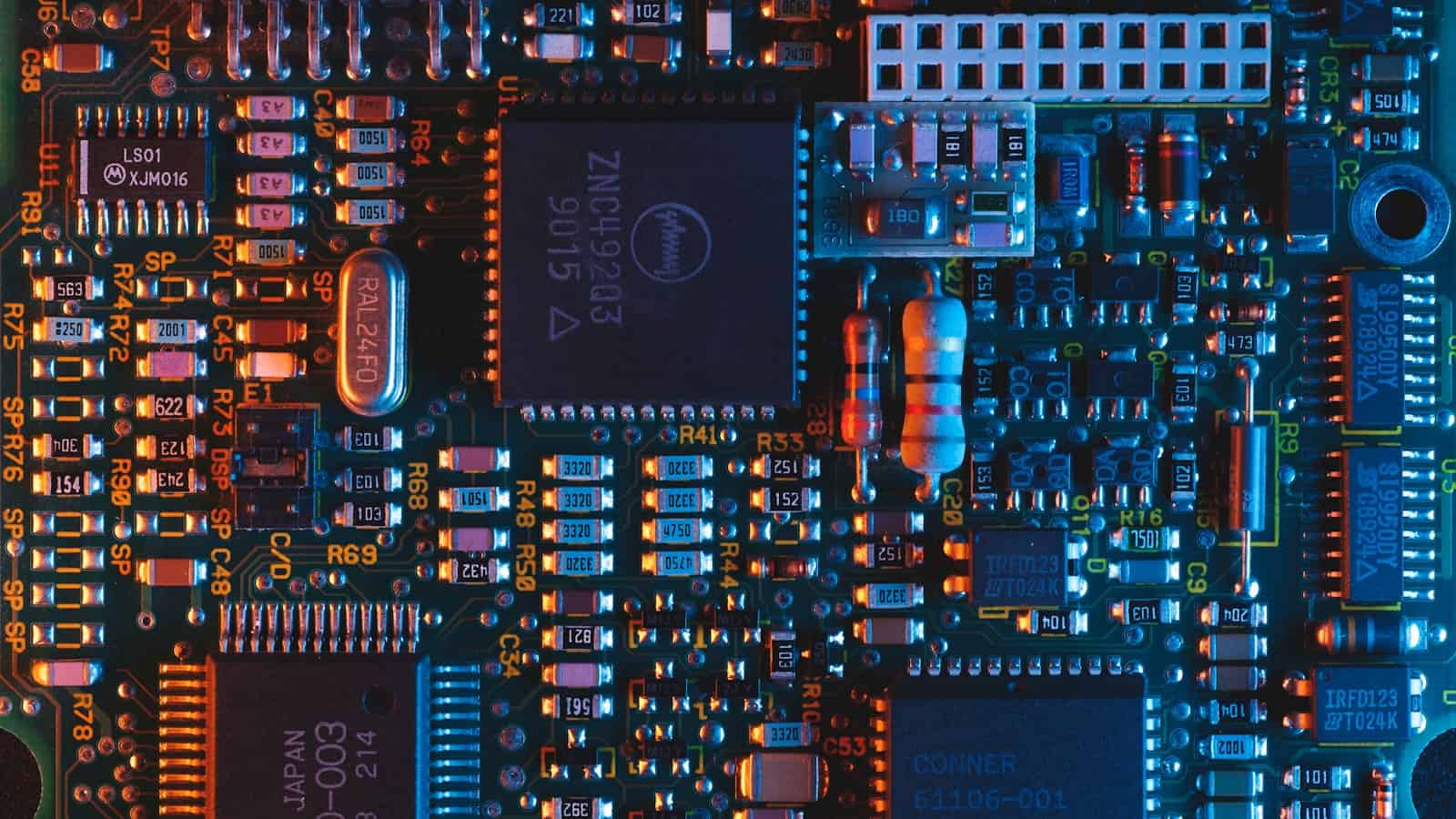
What is EMS PCB ?
Posted by
–
Read more: What is EMS PCB ?Introduction to EMS PCB EMS PCB stands for Electronics Manufacturing Services for Printed Circuit Boards. It refers to the end-to-end services provided by electronics contract manufacturers to design, produce, assemble, and test PCB-based products for Original Equipment Manufacturers (OEMs). EMS providers offer a wide range of services including: PCB design and layout Prototyping Component sourcing…
-
What is the thickest copper PCB?
Posted by
–
 Read more: What is the thickest copper PCB?
Introduction to Heavy Copper PCBs Heavy copper PCBs, also known as thick copper PCBs, are printed circuit boards that feature copper traces and planes significantly thicker than those found in standard PCBs. These boards are designed to handle high currents, provide better heat dissipation, and offer increased mechanical stability. Heavy copper PCBs are essential for…
-
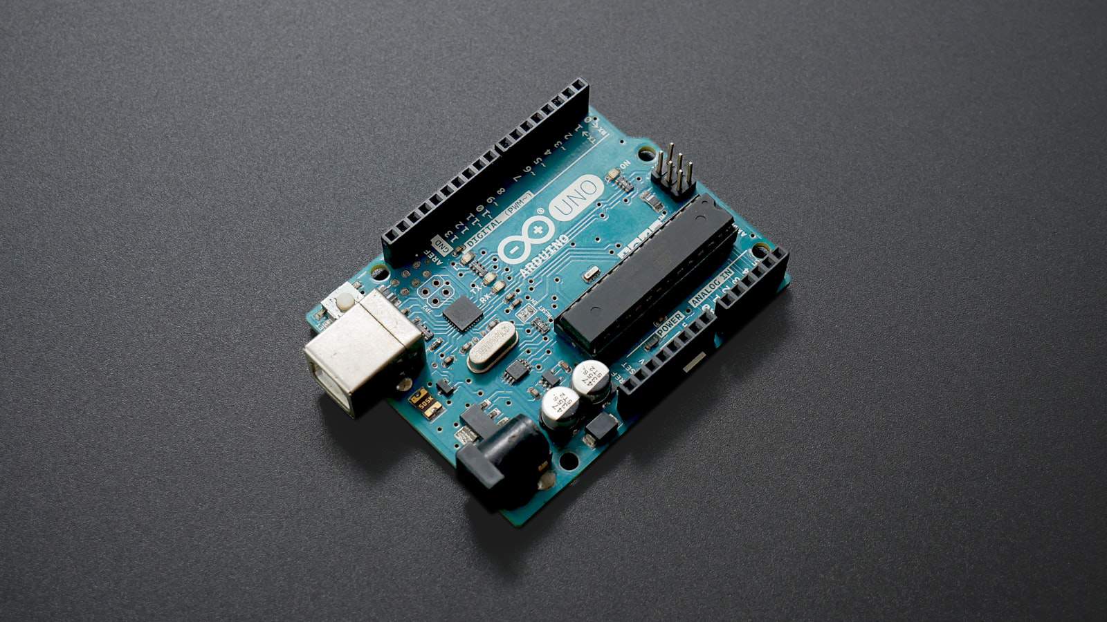
How to make a microcontroller PCB?
Posted by
–
 Read more: How to make a microcontroller PCB?
Choosing the Right Microcontroller The first step in creating a microcontroller PCB is selecting the appropriate microcontroller for your project. There are numerous options available, each with its own features, capabilities, and price points. Some popular microcontroller families include: Arduino (ATmega) PIC (Microchip) STM32 (ST Microelectronics) ESP32 (Espressif Systems) When choosing a microcontroller, consider factors…
-
What is V-groove in PCB?
Posted by
–
 Read more: What is V-groove in PCB?
Introduction to V-groove PCB Technology V-groove PCB, also known as v-scoring or v-cut PCB, is an advanced printed circuit board fabrication technique that involves cutting V-shaped grooves partially through the board substrate. This process enables the creation of clean, precise break-away tabs, making it easier to separate individual boards from a larger panel. V-groove technology…
-
What are PTH / NPTH holes in PCB?
Posted by
–
 Read more: What are PTH / NPTH holes in PCB?
What are PTH holes in PCB? PTH (Plated Through Hole) refers to holes in a PCB that have been electroplated with a conductive material, typically copper. The plating process creates an electrical connection between the top and bottom layers of the PCB, allowing components to be soldered on both sides of the board. PTH holes…
-
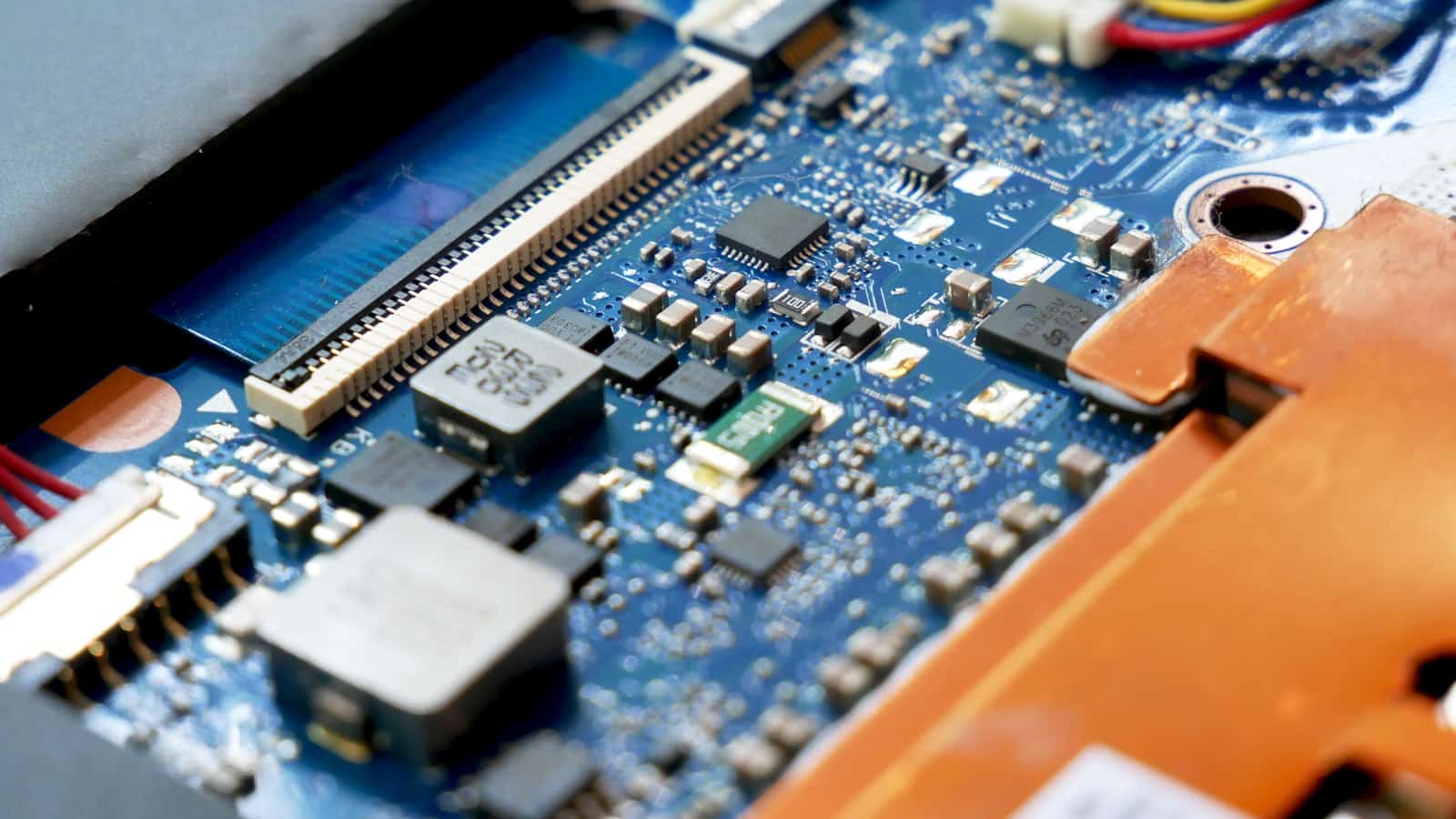
What is an embedded PCB?
Posted by
–
 Read more: What is an embedded PCB?
The Role of Embedded PCBs in Modern Electronics Embedded PCBs play a crucial role in the functionality and performance of modern electronic devices. They are responsible for interconnecting various components, such as microprocessors, memory chips, sensors, and communication modules, enabling them to work together seamlessly. The compact and efficient design of embedded PCBs allows for…
-
 Read more: Top Quality 8 Layer PCB Stackup Manufacturer and Supplier
What is an 8 Layer PCB? An 8 layer printed circuit board (PCB) is a complex, multi-layered board that consists of eight conductive copper layers laminated together with insulating material. These layers are interconnected through carefully designed vias and plated through-holes (PTHs) to create intricate circuits capable of handling high-speed signals and dense component placement.…
-
 Read more: What is Back Drilling in PCB Design and Manufacturing?
Understanding the Concept of Stub Resonance in PCBs Before we explore back drilling, it is essential to understand the concept of stub resonance in PCBs. In multi-layer PCBs, signal vias are used to connect traces on different layers. However, these vias often extend beyond the target layer, creating an unused portion known as a stub.…
-
What is the CTI value in PCB?
Posted by
–
 Read more: What is the CTI value in PCB?
Introduction to CTI Value in PCB In the world of printed circuit board (PCB) manufacturing, various factors contribute to the overall quality and reliability of the final product. One critical aspect that designers and manufacturers need to consider is the Comparative Tracking Index (CTI) value. The CTI value is a measure of a material’s ability…
-
2+N+2 PCB Stackup Design for HDI Boards
Posted by
–
 Read more: 2+N+2 PCB Stackup Design for HDI Boards
What is a 2+N+2 PCB Stackup? A 2+N+2 PCB stackup is a specific arrangement of layers in an HDI PCB, where “2” represents the number of outer layers (top and bottom), “N” represents the number of inner layers, and the second “2” represents the two additional layers used for power and ground planes. This stackup…


