
PCB Assembly Blog
-
Embedded World 2024 – Your Personal Ticket
Posted by
–
Read more: Embedded World 2024 – Your Personal TicketIntroduction to Embedded World 2024 Embedded World is the world’s leading trade fair for embedded systems, showcasing the latest trends, innovations, and technologies in the field. The event attracts a wide range of professionals, including developers, designers, product managers, and decision-makers from various industries such as automotive, industrial, medical, and […]
-
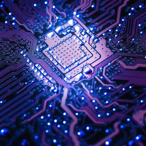 Read more: 10 Rules for Better Data – Avoid PCB Design Issues
Rule 1: Establish a Clear and Consistent Naming Convention A clear and consistent naming convention is essential for effective data management in PCB Design. This includes naming conventions for files, folders, components, and nets. By establishing a standardized naming convention, you can: Improve communication among team members Reduce the risk […]
-
Blind and Buried Vias
Posted by
–
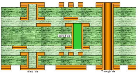 Read more: Blind and Buried Vias
What are Blind Vias? Blind vias are a type of interconnection used in multi-layer PCBs, where the via starts on an outer layer and terminates on an inner layer, without going through the entire board. Unlike through-hole vias, which are visible on both sides of the PCB, blind vias are […]
-
What is Spring-loaded Pins
Posted by
–
 Read more: What is Spring-loaded Pins
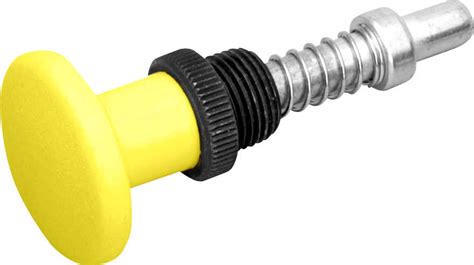
What are Spring-loaded Pins? Spring-loaded pins are electrical connectors that consist of a cylindrical pin and a spring mechanism. The pin is typically made of a conductive material, such as brass or beryllium copper, and is plated with gold, silver, or other metals to enhance conductivity and durability. The spring […]
-
Copper Distribution on a Panel
Posted by
–
 Read more: Copper Distribution on a Panel
Introduction to Copper Panels and Their Importance Copper panels are widely used in various industries due to their excellent electrical and thermal conductivity, corrosion resistance, and durability. These panels play a crucial role in the manufacturing of electronic devices, printed circuit boards (PCBs), and other applications where efficient heat dissipation […]
-
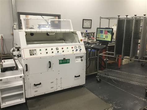
 Read more: Placer camera-assisted manual pick and place machine
Introduction to Placer-assisted pick-and-place In the world of manufacturing and assembly, pick-and-place machines have become an essential tool for improving efficiency and accuracy. These machines are designed to pick up components from a specific location and place them onto a target area, such as a printed circuit board (PCB) or […]
-
Rayming-reflow-pilot door open
Posted by
–
 Read more: Rayming-reflow-pilot door open
Introduction to Rayming-reflow-pilot The Rayming-reflow-pilot is a groundbreaking technology in the field of Surface Mount Technology (SMT) soldering. This innovative system has opened new doors for manufacturers, enabling them to achieve higher efficiency, precision, and reliability in their soldering processes. With its advanced features and user-friendly interface, the Rayming-reflow-pilot is […]
-
Selective Soldering
Posted by
–
 Read more: Selective Soldering
What is Selective Soldering? Selective soldering is a process used in electronics manufacturing to solder specific components to a PCB-Assembly.com/printed-circuit-board/”>printed circuit board (PCB) using a precisely controlled solder fountain or mini wave. Unlike wave soldering, which solders all components on a PCB simultaneously, selective soldering targets only the desired through-hole […]
-
What is Pad to Pad (PP)?
Posted by
–
 Read more: What is Pad to Pad (PP)?
Why is Pad to Pad Spacing Important? Proper Pad to Pad (PP) spacing is essential for several reasons: 1. Manufacturability Adequate spacing between pads allows for reliable soldering of components to the PCB. If pads are too close together, there is a risk of solder bridges forming, causing short circuits […]
-
What is Via Filling?
Posted by
–
 Read more: What is Via Filling?
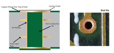
How Does ViaFilling Work? The ViaFilling process typically involves the following steps: Drilling: Small holes, known as vias, are drilled through the PCB substrate to create electrical connections between different layers. Cleaning: The drilled vias are cleaned to remove any debris or contaminants that may interfere with the filling process. […]


