What is Bare Board Testing?
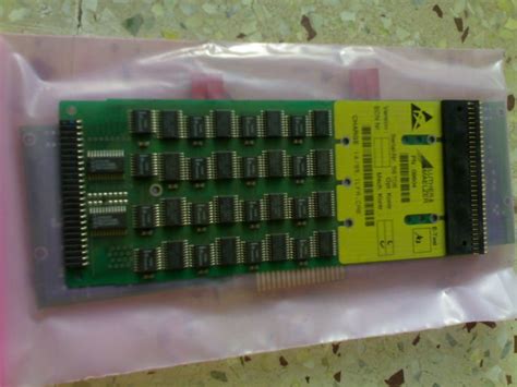
Bare board testing, also known as printed circuit board (PCB) testing, is a crucial step in the manufacturing process of electronic devices. It involves testing the PCB before any components are mounted on it to ensure that it functions as intended and meets the required specifications. This testing process helps identify defects, short circuits, open circuits, and other issues that may affect the performance of the final product.
Types of Bare Board Testing
There are several types of bare board testing methods, each with its own advantages and limitations. Some of the most common types include:
-
Visual Inspection: This is the most basic form of bare board testing, where the PCB is visually inspected for any obvious defects, such as scratches, cracks, or discoloration.
-
Automated Optical Inspection (AOI): AOI uses high-resolution cameras and image processing software to detect surface-level defects, such as missing or misaligned traces, solder bridges, and incorrect component placement.
-
In-Circuit Testing (ICT): ICT involves using a bed-of-nails fixture to make electrical contact with specific points on the PCB and test for short circuits, open circuits, and other issues.
-
Flying Probe Testing: This method uses a set of movable probes to make contact with various points on the PCB and test for electrical continuity and other parameters.
-
Boundary Scan Testing: Also known as JTAG testing, this method uses a special test access port (TAP) to test the interconnections between integrated circuits on the PCB.
Benefits of Bare Board Testing
Bare board testing offers several benefits, including:
-
Early Detection of Defects: By identifying defects early in the manufacturing process, bare board testing can help prevent costly rework and delays later on.
-
Improved Quality: Bare board testing helps ensure that the PCB meets the required specifications and functions as intended, resulting in higher-quality end products.
-
Reduced Manufacturing Costs: By catching defects early, bare board testing can help reduce the overall manufacturing costs associated with rework and scrap.
-
Faster Time-to-Market: Bare board testing can help streamline the manufacturing process and reduce the time required to bring a product to market.
The Bare Board Testing Process
The bare board testing process typically involves the following steps:
-
PCB Design Review: Before testing begins, the PCB design is reviewed to ensure that it meets the required specifications and is suitable for testing.
-
Test Fixture Design: Based on the PCB design, a test fixture is designed to facilitate the testing process. This fixture may include a bed-of-nails, flying probes, or other contact methods.
-
Test Program Development: A test program is developed to define the specific tests that will be performed on the PCB, including continuity, isolation, and other electrical parameters.
-
PCB Loading: The PCB is loaded into the test fixture, ensuring proper alignment and contact with the test probes.
-
Test Execution: The test program is executed, and the results are recorded and analyzed to identify any defects or issues.
-
Reporting and Documentation: A detailed report is generated, documenting the test results, any defects found, and the overall quality of the PCB.
Test Fixture Design Considerations
Designing an effective test fixture is crucial for accurate and reliable bare board testing. Some key considerations include:
-
Contact Method: The choice of contact method (e.g., bed-of-nails, flying probes) depends on factors such as the PCB layout, component density, and test requirements.
-
Probe Placement: Probes must be placed accurately to ensure proper contact with the PCB test points and avoid damage to the board.
-
Fixture Rigidity: The test fixture must be rigid enough to maintain proper alignment and contact pressure throughout the testing process.
-
Accessibility: The test fixture should provide easy access to the PCB for loading and unloading, as well as for maintenance and repair.
Test Program Development
Developing an effective test program is essential for thorough and accurate bare board testing. Some key considerations include:
-
Test Coverage: The test program should cover all relevant electrical parameters, such as continuity, isolation, and resistance, to ensure comprehensive testing.
-
Test Limits: Appropriate test limits must be defined based on the PCB specifications and tolerances to accurately identify defects and issues.
-
Test Sequence: The test sequence should be optimized to minimize testing time while ensuring thorough coverage of all test points.
-
Test Automation: Automated test programs can help improve testing efficiency and repeatability, reducing the potential for human error.

Advantages of Automated Bare Board Testing
Automated bare board testing offers several advantages over manual testing methods, including:
-
Increased Speed: Automated testing systems can perform tests much faster than manual methods, significantly reducing overall testing time.
-
Improved Accuracy: Automated systems can maintain consistent test conditions and eliminate human error, resulting in more accurate and reliable test results.
-
Higher Repeatability: Automated testing ensures that the same tests are performed consistently across multiple PCBs, improving repeatability and reducing variability.
-
Reduced Labor Costs: Automated testing requires less human intervention, reducing labor costs associated with manual testing methods.
Automated Optical Inspection (AOI)
AOI is a popular automated bare board testing method that uses high-resolution cameras and image processing software to detect surface-level defects. Some key advantages of AOI include:
-
Fast Inspection Speed: AOI systems can inspect PCBs at a much higher speed compared to manual visual inspection, significantly reducing testing time.
-
High Detection Accuracy: Advanced image processing algorithms enable AOI systems to detect even the smallest defects with high accuracy.
-
Consistent Results: AOI systems maintain consistent inspection conditions, ensuring repeatable and reliable test results.
-
Reduced Human Error: By automating the inspection process, AOI minimizes the potential for human error and subjectivity.
In-Circuit Testing (ICT)
ICT is another widely used automated bare board testing method that involves using a bed-of-nails fixture to make electrical contact with specific points on the PCB. Some key advantages of ICT include:
-
Comprehensive Testing: ICT can test a wide range of electrical parameters, including continuity, isolation, and component values, providing thorough coverage of the PCB.
-
High Fault Coverage: ICT can detect a high percentage of potential faults, ensuring that defective PCBs are identified and removed from the production process.
-
Fast Testing Speed: ICT systems can perform tests quickly, allowing for high throughput and reduced overall testing time.
-
Automated Reporting: ICT systems generate detailed test reports automatically, simplifying documentation and analysis of test results.

Challenges and Limitations of Bare Board Testing
Despite its many benefits, bare board testing also presents some challenges and limitations, including:
-
Test Access: As PCBs become more complex and densely populated with components, providing adequate test access can be challenging, requiring careful design of test fixtures and probe placement.
-
High-Frequency Circuits: Testing high-frequency circuits can be difficult due to signal integrity issues and the need for specialized test equipment and techniques.
-
Cost: Automated bare board testing systems can be expensive, requiring significant upfront investment in equipment, fixtures, and software.
-
Limited Defect Detection: While bare board testing can identify many types of defects, it may not detect all issues, particularly those related to component functionality or performance.
Overcoming Challenges in Bare Board Testing
To overcome these challenges and limitations, manufacturers can employ various strategies, such as:
-
Design for Testability (DFT): Incorporating testability features into the PCB design, such as test points and boundary scan architecture, can improve test access and coverage.
-
Advanced Testing Techniques: Using specialized testing methods, such as high-frequency probing and capacitance testing, can help address the challenges associated with testing high-frequency circuits.
-
Collaborative Design Process: Close collaboration between PCB designers, test engineers, and manufacturing teams can help optimize the PCB design for testability and manufacturability, reducing testing challenges and costs.
-
Complementary Testing Methods: Combining bare board testing with other testing methods, such as functional testing and burn-in testing, can help provide a more comprehensive assessment of the PCB’s performance and reliability.

Future Trends in Bare Board Testing
As electronic devices continue to evolve and become more complex, bare board testing methods must adapt to keep pace with these changes. Some key trends shaping the future of bare board testing include:
-
Increased Automation: The ongoing development of more advanced and intelligent automated testing systems will further improve testing speed, accuracy, and efficiency.
-
Integrated Testing Solutions: The integration of multiple testing methods, such as AOI, ICT, and functional testing, into a single platform will provide a more comprehensive and streamlined testing process.
-
Adaptive Testing: The use of adaptive testing techniques, which adjust the test sequence and parameters based on real-time results, will enable more efficient and targeted testing.
-
Big Data and Analytics: The growing use of data analytics and machine learning will enable manufacturers to leverage test data for process optimization, yield improvement, and predictive maintenance.
The Role of Industry Standards in Bare Board Testing
Industry standards play a crucial role in ensuring the quality, reliability, and consistency of bare board testing. Some key standards include:
-
IPC-9252A: This standard provides guidelines for the electrical testing of unpopulated printed boards, including test methods, fixtures, and reporting requirements.
-
IPC-A-600: This standard defines the acceptability criteria for printed circuit boards, including visual inspection requirements and defect classifications.
-
ISO 9001: This international standard specifies requirements for a quality management system, helping ensure that manufacturers consistently provide products that meet customer and regulatory requirements.
Adhering to these and other relevant industry standards helps manufacturers maintain high quality standards, reduce defects, and improve customer satisfaction.
Frequently Asked Questions (FAQ)
-
What is the difference between bare board testing and functional testing?
Bare board testing focuses on testing the unpopulated PCB for defects and ensuring that it meets the required electrical specifications. Functional testing, on the other hand, involves testing the fully assembled PCB with all components mounted to verify that it functions as intended in the final product. -
How does bare board testing help reduce manufacturing costs?
By identifying defects early in the manufacturing process, bare board testing helps prevent costly rework and scrap later on. This early detection of issues allows manufacturers to address problems before they escalate, ultimately reducing overall manufacturing costs. -
What are some common defects that bare board testing can detect?
Bare board testing can detect a wide range of defects, including short circuits, open circuits, incorrect trace widths, missing or excess copper, and incorrect hole sizes. It can also identify issues related to electrical continuity, isolation, and resistance. -
How often should bare board testing be performed during the manufacturing process?
The frequency of bare board testing depends on factors such as the complexity of the PCB, the production volume, and the specific quality control requirements. In general, bare board testing should be performed on a sample basis at various stages of the manufacturing process, such as after PCB fabrication and before component assembly. -
Can bare board testing completely eliminate the need for functional testing?
While bare board testing is an essential part of the quality control process, it cannot completely replace functional testing. Bare board testing focuses on the electrical characteristics of the unpopulated PCB, while functional testing verifies the performance of the fully assembled board with all components in place. Both types of testing are necessary to ensure the overall quality and reliability of the final product.
Conclusion
Bare board testing is a critical step in the manufacturing process of electronic devices, helping ensure the quality, reliability, and performance of printed circuit boards. By identifying defects and issues early in the production cycle, bare board testing helps reduce manufacturing costs, improve product quality, and accelerate time-to-market.
As PCBs continue to become more complex and densely populated, the importance of effective bare board testing methods will only continue to grow. By staying up-to-date with the latest testing technologies, techniques, and industry standards, manufacturers can overcome the challenges associated with bare board testing and deliver high-quality products that meet the evolving needs of their customers.


Leave a Reply