Introduction to PCB-CarbonContacts
Printed circuit boards (PCBs) are essential components in modern electronics, providing a platform for interconnecting electronic components. One critical aspect of PCB design and manufacturing is the application of contacts, which enable electrical connections between the PCB and other components or devices. Among the various materials used for PCB contacts, carbon has emerged as a promising option due to its unique properties and advantages. In this article, we will explore the process of applying carbon contacts to PCBs, discussing the benefits, techniques, and considerations involved.
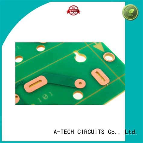
What are Carbon Contacts?
Carbon contacts are electrical contacts made from carbon materials, such as graphite or carbon nanotubes. These contacts offer several advantages over traditional metal contacts, including:
- High electrical conductivity
- Excellent thermal stability
- Low contact resistance
- Resistance to oxidation and corrosion
- Compatibility with a wide range of substrate materials
Advantages of Using Carbon Contacts in PCBs
The use of carbon contacts in PCBs offers several benefits that make them an attractive choice for various applications. Some of the key advantages include:
-
Improved Signal Integrity: Carbon contacts exhibit low contact resistance, which helps in reducing signal loss and improving overall signal integrity in high-frequency applications.
-
Enhanced Durability: Carbon contacts are resistant to oxidation and corrosion, making them more durable than metal contacts in harsh environments or under prolonged use.
-
Reduced Electromagnetic Interference (EMI): The inherent properties of carbon materials help in reducing EMI, which is crucial in sensitive electronic devices and systems.
-
Compatibility with Diverse Substrates: Carbon contacts can be applied to a wide range of PCB substrate materials, including flexible substrates, making them versatile for various applications.
Techniques for Applying Carbon Contacts to PCBs
There are several techniques used for applying carbon contacts to PCBs, each with its own advantages and considerations. Let’s explore some of the commonly used methods:
1. Screen Printing
Screen printing is a popular technique for applying carbon contacts to PCBs. It involves the following steps:
- Preparing a stencil or screen with the desired contact pattern
- Applying a carbon paste or ink onto the PCB surface through the stencil
- Curing the printed contacts using heat or ultraviolet (UV) light
Screen printing offers several advantages, such as:
- High throughput and efficiency for large-scale production
- Ability to create complex contact patterns with fine features
- Compatibility with a range of carbon materials and PCB substrates
However, screen printing also has some limitations, including:
- Potential for variations in contact thickness and uniformity
- Need for careful control of printing parameters to ensure consistent results
2. Inkjet Printing
Inkjet printing is a digital printing technique that allows for precise deposition of carbon contacts onto PCBs. The process involves:
- Formulating a carbon-based ink with suitable rheological properties
- Loading the ink into an inkjet printer cartridge
- Printing the contacts onto the PCB surface using a computer-controlled printer head
- Sintering or curing the printed contacts to improve their electrical and mechanical properties
Inkjet printing offers several benefits, such as:
- High precision and resolution for creating fine contact features
- Ability to print on irregular or curved PCB surfaces
- Reduced material waste compared to screen printing
- Flexibility in design changes and customization
However, inkjet printing also has some challenges, including:
- Potential for nozzle clogging and printing inconsistencies
- Limited throughput compared to screen printing
- Need for specialized inks and printing equipment
3. Aerosol Jet Printing
Aerosol jet printing is an advanced technique for applying carbon contacts to PCBs, offering high precision and resolution. The process involves:
- Creating an aerosol of carbon-based ink using an atomizer
- Focusing the aerosol stream onto the PCB surface using a sheath gas
- Depositing the carbon contacts in a computer-controlled manner
- Sintering or curing the printed contacts
Aerosol jet printing offers several advantages, such as:
- Ability to create extremely fine contact features (down to 10 microns)
- Compatibility with a wide range of carbon materials and PCB substrates
- Reduced overspray and material waste compared to other printing techniques
- Flexibility in printing on non-planar surfaces
However, aerosol jet printing also has some limitations, including:
- Higher equipment and operating costs compared to other techniques
- Need for specialized inks and substrate preparation
- Potential for nozzle clogging and process variability

Considerations for Applying Carbon Contacts to PCBs
When applying carbon contacts to PCBs, several factors need to be considered to ensure optimal performance and reliability. Some of the key considerations include:
-
Material Selection: Choosing the appropriate carbon material based on the specific application requirements, such as electrical conductivity, thermal stability, and compatibility with the PCB substrate.
-
Surface Preparation: Ensuring proper cleaning and treatment of the PCB surface before applying carbon contacts to enhance adhesion and electrical contact.
-
Contact Design: Optimizing the contact pattern and dimensions to achieve the desired electrical and mechanical properties, considering factors such as current carrying capacity, contact resistance, and mechanical stability.
-
Printing Parameters: Controlling the printing process parameters, such as ink viscosity, printing speed, and curing conditions, to achieve consistent and reliable contact formation.
-
Post-Processing: Applying appropriate post-processing techniques, such as sintering or coating, to improve the electrical and mechanical properties of the carbon contacts.

Applications of Carbon Contacts in PCBs
Carbon contacts find applications in various fields where PCBs are used, including:
-
Electronics: Carbon contacts are used in PCBs for electronic devices, such as sensors, displays, and wearable electronics, where high conductivity and durability are required.
-
Automotive: In the automotive industry, carbon contacts are used in PCBs for various applications, such as engine control units, infotainment systems, and advanced driver assistance systems (ADAS).
-
Aerospace: Carbon contacts are used in PCBs for aerospace applications, such as avionics, satellite communication systems, and radar systems, where high reliability and performance are critical.
-
Medical Devices: In the medical device industry, carbon contacts are used in PCBs for applications such as biosensors, wearable health monitors, and implantable devices, where biocompatibility and long-term stability are essential.
-
Flexible Electronics: Carbon contacts are suitable for use in flexible PCBs, enabling the development of bendable and stretchable electronic devices for various applications, such as wearables, displays, and sensors.

Frequently Asked Questions (FAQ)
-
Q: What are the main advantages of using carbon contacts in PCBs compared to traditional metal contacts?
A: Carbon contacts offer several advantages over metal contacts, including high electrical conductivity, excellent thermal stability, low contact resistance, resistance to oxidation and corrosion, and compatibility with a wide range of substrate materials. -
Q: What are the common techniques used for applying carbon contacts to PCBs?
A: The common techniques used for applying carbon contacts to PCBs include screen printing, inkjet printing, and aerosol jet printing. Each technique has its own advantages and considerations, such as throughput, precision, and material compatibility. -
Q: Can carbon contacts be applied to flexible PCBs?
A: Yes, carbon contacts can be applied to flexible PCBs, making them suitable for use in bendable and stretchable electronic devices. The compatibility of carbon contacts with flexible substrates expands their application range to wearables, displays, and sensors. -
Q: What factors should be considered when selecting a carbon material for PCB contacts?
A: When selecting a carbon material for PCB contacts, factors such as electrical conductivity, thermal stability, and compatibility with the PCB substrate should be considered. The specific application requirements will guide the selection of the most appropriate carbon material. -
Q: Are there any post-processing techniques applied to carbon contacts after printing?
A: Yes, post-processing techniques such as sintering or coating can be applied to improve the electrical and mechanical properties of the carbon contacts. These techniques help in enhancing the conductivity, adhesion, and durability of the contacts.
Conclusion
Applying carbon contacts to PCBs offers numerous benefits, including improved signal integrity, enhanced durability, reduced electromagnetic interference, and compatibility with diverse substrates. Various techniques, such as screen printing, inkjet printing, and aerosol jet printing, can be used to apply carbon contacts, each with its own advantages and considerations. When implementing carbon contacts in PCBs, factors such as material selection, surface preparation, contact design, printing parameters, and post-processing should be carefully considered to ensure optimal performance and reliability.
As the demand for high-performance and reliable electronic devices continues to grow, the use of carbon contacts in PCBs is expected to increase across various industries, including electronics, automotive, aerospace, medical devices, and flexible electronics. With ongoing research and advancements in carbon-based materials and printing technologies, the potential for carbon contacts in PCBs is vast, opening up new possibilities for innovative and advanced electronic applications.


Leave a Reply