Introduction to Microwave PCBs
A microwave printed circuit board (PCB) is a specialized type of PCB designed to operate at high frequencies, typically in the microwave frequency range (300 MHz to 300 GHz). These PCBs are used in various applications, such as telecommunications, radar systems, satellite communications, and wireless networking equipment. Microwave PCBs require specific design considerations and manufacturing techniques to ensure optimal performance and reliability at these high frequencies.
Key Characteristics of Microwave PCBs
- High-frequency operation
- Specialized substrate materials
- Controlled impedance
- Minimized signal loss and distortion
- Careful layout and routing
Substrate Materials for Microwave PCBs
The choice of substrate material is crucial for microwave PCBs, as it directly affects the board’s performance at high frequencies. Some common substrate materials used in microwave PCB fabrication include:
PTFE (Polytetrafluoroethylene)
PTFE, also known as Teflon, is a popular choice for microwave PCBs due to its excellent electrical properties and low dielectric loss. It has a stable dielectric constant over a wide frequency range and maintains its properties at high temperatures.
Rogers Materials
Rogers Corporation offers a range of high-performance substrate materials specifically designed for microwave applications. Some popular Rogers materials include:
- RO4000 series: A hydrocarbon ceramic laminate with low dielectric loss and good thermal stability.
- RO3000 series: A ceramic-filled PTFE composite with low dielectric loss and good mechanical properties.
- RT/duroid: A PTFE-based laminate with low dielectric loss and good thermal stability.
Isola Materials
Isola Group also provides a variety of substrate materials suitable for microwave PCBs, such as:
- I-Tera MT40: A low-loss, high-performance laminate with a stable dielectric constant and good thermal properties.
- Astra MT77: A low-loss, high-speed laminate with excellent electrical performance and reliability.
Controlled Impedance in Microwave PCBs
Maintaining controlled impedance is essential in microwave PCB design to ensure proper signal integrity and minimize reflections. The characteristic impedance of a transmission line is determined by factors such as the substrate material, trace width, trace thickness, and the distance between the trace and the reference plane.
Impedance Matching Techniques
To achieve controlled impedance, designers use various techniques, such as:
- Microstrip lines: A transmission line consisting of a conductive trace on one side of the substrate, with a ground plane on the other side.
- Striplines: A transmission line sandwiched between two ground planes, providing better shielding and reduced radiation compared to microstrip lines.
- Coplanar waveguides: A transmission line with a conductive trace and two ground planes on the same side of the substrate, offering low dispersion and good impedance control.
Impedance Calculation and Simulation
To determine the appropriate trace dimensions and spacing for a given characteristic impedance, designers use impedance calculation tools and electromagnetic simulation software. These tools help optimize the PCB layout and ensure that the desired impedance is maintained throughout the board.

Signal Integrity Considerations
Signal integrity is a critical aspect of microwave PCB design, as high-frequency signals are more susceptible to loss, distortion, and interference. Some key signal integrity considerations include:
Minimizing Signal Loss
Signal loss in microwave PCBs can be minimized by:
- Choosing low-loss substrate materials
- Minimizing trace lengths and using smooth, gradual bends
- Using wider traces to reduce resistive losses
- Employing ground planes and proper shielding to reduce radiation and crosstalk
Reducing Discontinuities
Discontinuities in the signal path can cause reflections and distortions, leading to signal degradation. To minimize discontinuities, designers should:
- Avoid abrupt changes in trace width or direction
- Use smooth, tapered transitions between different trace widths
- Minimize the use of vias, and when necessary, use controlled-depth vias or blind/buried vias
- Employ proper termination techniques to reduce reflections
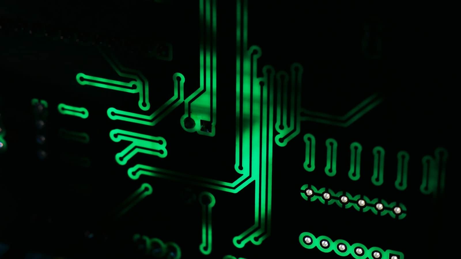
Layout and Routing Techniques
Proper layout and routing are essential for optimal performance in microwave PCBs. Some best practices include:
Component Placement
- Place components close to their associated traces to minimize trace lengths
- Group components with similar functions together to reduce interference
- Consider the component orientation and placement for optimal signal flow
Trace Routing
- Route traces as straight as possible, minimizing bends and turns
- Use smooth, gradual bends instead of sharp corners
- Maintain consistent trace widths and spacings to ensure controlled impedance
- Avoid running traces parallel to each other for long distances to minimize crosstalk
Ground Planes and Shielding
- Use uninterrupted ground planes to provide a low-impedance return path and reduce radiation
- Employ proper shielding techniques, such as grounded guard traces or metallic enclosures, to minimize interference and crosstalk
- Use stitching vias to connect ground planes on different layers and improve shielding effectiveness
Manufacturing Considerations
Manufacturing microwave PCBs requires specialized techniques and processes to ensure high-quality and reliable boards. Some key manufacturing considerations include:
Material Handling and Processing
- Use clean, dust-free environments to prevent contamination of the substrate materials
- Handle materials carefully to avoid damage or deformation
- Follow proper lamination and curing processes to ensure consistent material properties
Etching and Plating
- Use high-resolution etching processes to achieve precise trace geometries
- Employ smooth, uniform plating to maintain consistent trace thickness and impedance
- Regularly monitor and control the etching and plating processes to ensure consistency and quality
Inspection and Testing
- Perform visual inspections to identify any defects or irregularities in the PCB
- Use automated optical inspection (AOI) systems to detect manufacturing defects
- Conduct electrical testing, such as time-domain reflectometry (TDR) or vector network analyzer (VNA) measurements, to verify signal integrity and performance
Applications of Microwave PCBs
Microwave PCBs find applications in various industries and products, including:
- Telecommunications: Cellular base stations, satellite communication systems, and wireless backhaul equipment
- Radar systems: Automotive radar, weather radar, and military radar applications
- Aerospace and defense: Avionics, missile guidance systems, and electronic warfare equipment
- Wireless networking: Wi-Fi routers, wireless access points, and point-to-point links
- Medical devices: Microwave ablation systems, imaging equipment, and wireless monitoring devices
Future Trends in Microwave PCB Technology
As the demand for higher data rates, increased bandwidth, and miniaturization continues to grow, microwave PCB technology is expected to evolve to meet these challenges. Some future trends in microwave PCB technology include:
- Advanced substrate materials: Development of new, low-loss substrate materials with improved electrical and thermal properties
- 3D printing: Adoption of 3D printing technologies for rapid prototyping and customized microwave components
- Integrated active components: Integration of active components, such as amplifiers and switches, directly onto the PCB to reduce size and improve performance
- Higher frequencies: Extending the operating frequency range of microwave PCBs to millimeter-wave and terahertz frequencies for emerging applications
- Increased use of simulation tools: Wider adoption of advanced electromagnetic simulation tools to optimize PCB designs and predict performance
Conclusion
Microwave PCBs are essential components in many modern electronic systems, enabling high-frequency communication and sensing applications. Designing and manufacturing these specialized PCBs requires careful consideration of substrate materials, controlled impedance, signal integrity, and layout techniques. As technology continues to advance, microwave PCBs will play an increasingly important role in shaping the future of wireless communications and other high-frequency applications.
Frequently Asked Questions (FAQ)
1. What is the difference between a microwave PCB and a regular PCB?
A microwave PCB is specifically designed to operate at high frequencies, typically in the microwave frequency range (300 MHz to 300 GHz). It requires specialized substrate materials, controlled impedance, and careful layout techniques to ensure optimal performance and signal integrity. In contrast, a regular PCB operates at lower frequencies and may not require the same level of design considerations.
2. What are the most common substrate materials used in microwave PCBs?
Some of the most common substrate materials used in microwave PCBs include PTFE (Polytetrafluoroethylene), Rogers materials (such as RO4000 and RO3000 series), and Isola materials (such as I-Tera MT40 and Astra MT77). These materials are chosen for their low dielectric loss, stable dielectric constant, and good thermal properties.
3. Why is controlled impedance important in microwave PCB design?
Controlled impedance is crucial in microwave PCB design to ensure proper signal integrity and minimize reflections. By maintaining a consistent characteristic impedance throughout the transmission lines, designers can reduce signal distortions, reflections, and power loss, ensuring optimal performance of the microwave circuit.
4. What are some techniques used to minimize signal loss in microwave PCBs?
To minimize signal loss in microwave PCBs, designers can employ several techniques, such as using low-loss substrate materials, minimizing trace lengths, using wider traces to reduce resistive losses, and employing ground planes and proper shielding to reduce radiation and crosstalk. Additionally, using smooth, gradual bends in traces and avoiding abrupt changes in trace geometry can help minimize signal loss.
5. How do manufacturing processes differ for microwave PCBs compared to regular PCBs?
Manufacturing microwave PCBs requires specialized techniques and processes to ensure high-quality and reliable boards. This includes using clean, dust-free environments to prevent contamination of substrate materials, employing high-resolution etching processes to achieve precise trace geometries, and conducting thorough inspections and electrical testing to verify signal integrity and performance. Manufacturers must also follow proper material handling, lamination, and curing processes to maintain consistent material properties throughout the production process.


Leave a Reply