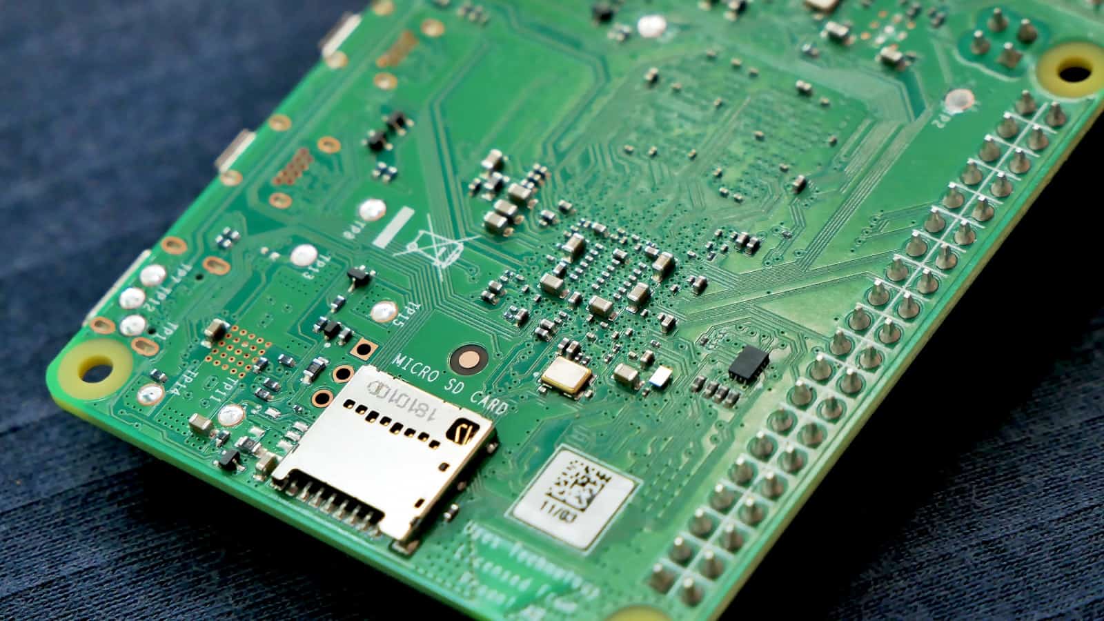
Introduction to PCB Depaneling
Printed Circuit Board (PCB) manufacturing often involves producing multiple PCBs on a single panel to optimize production efficiency and minimize material waste. Once the fabrication and assembly processes are complete, the individual PCBs need to be separated from the panel. This process is known as PCB depaneling or singulation. Depaneling is a crucial step in the PCB manufacturing process, as it directly impacts the quality, functionality, and reliability of the final product.
What is PCB Panelization?
Before diving into the details of depaneling, it’s essential to understand PCB panelization. Panelization is the process of designing and fabricating multiple PCBs on a single, larger board called a panel. This approach allows manufacturers to produce several PCBs simultaneously, reducing production time and costs.
Advantages of PCB panelization include:
- Increased production efficiency
- Reduced material waste
- Simplified handling and assembly
- Improved consistency and uniformity
Types of PCB Panels
There are two main types of PCB panels:
-
Array Panels: In an array panel, multiple identical PCBs are arranged in a grid pattern. This type of panelization is suitable for high-volume production of the same PCB design.
-
Multi-Design Panels: A multi-design panel contains different PCB designs on a single panel. This approach is useful for low-volume production or prototyping, where various PCB designs are required in smaller quantities.
PCB Depaneling Methods
There are several methods used for PCB depaneling, each with its advantages and disadvantages. The choice of the depaneling method depends on factors such as the PCB material, thickness, component proximity to the board edge, and the required throughput. Let’s explore the most common PCB depaneling methods.
V-Scoring
V-scoring is a popular depaneling method that involves creating V-shaped grooves along the edges of the individual PCBs during the fabrication process. These grooves weaken the panel material, allowing the PCBs to be easily snapped apart by hand or with a simple tool.
Advantages of V-scoring:
- Cost-effective
- Simple process
- No additional equipment required
- Suitable for low-volume production
Disadvantages of V-scoring:
- Not suitable for thick PCBs or boards with components near the edges
- Risk of PCB damage during the snapping process
- Inconsistent break edges
- Not ideal for high-volume production
Tab Routing
Tab routing is another common depaneling method that uses a router to create small tabs connecting the individual PCBs to the panel frame. The tabs are designed to be strong enough to hold the PCBs securely during the assembly process but weak enough to be easily broken when the PCBs need to be separated.
Advantages of tab routing:
- Suitable for PCBs with components near the edges
- Provides a secure hold during the assembly process
- Allows for easier automation of the depaneling process
- Consistent break edges
Disadvantages of tab routing:
- Requires specialized routing equipment
- Increased material waste due to the tabs
- Risk of PCB damage during the breaking process
- Not suitable for very thin or fragile PCBs
Punch and Die Depaneling
Punch and die depaneling uses a custom-designed punch and die set to cut the individual PCBs from the panel. The punch and die are CNC machined to match the specific PCB layout, ensuring precise and clean cuts.
Advantages of punch and die depaneling:
- High precision and clean cuts
- Suitable for high-volume production
- Minimal stress on the PCBs during the depaneling process
- Can handle complex PCB shapes
Disadvantages of punch and die depaneling:
- High initial tooling costs for custom punch and die sets
- Not cost-effective for low-volume production or prototyping
- Limited flexibility for design changes
Laser Depaneling
Laser depaneling uses a high-power laser to cut the individual PCBs from the panel. This method offers high precision and minimal stress on the PCBs, making it suitable for sensitive components and fine-pitch designs.
Advantages of laser depaneling:
- High precision and clean cuts
- Minimal mechanical stress on the PCBs
- Suitable for sensitive components and fine-pitch designs
- Flexibility in cutting patterns and shapes
Disadvantages of laser depaneling:
- High equipment costs
- Slower process compared to other methods
- Potential for heat-affected zones (HAZ) on the PCB edges
- Not suitable for thick PCBs or boards with metallic substrates
Saw Depaneling
Saw depaneling uses a high-speed circular saw or a specialized PCB saw to cut the individual PCBs from the panel. This method is suitable for PCBs with thick substrates or those requiring straight, clean edges.
Advantages of saw depaneling:
- Suitable for thick PCBs and boards with metallic substrates
- Straight and clean edges
- Relatively high throughput
- Cost-effective for medium to high-volume production
Disadvantages of saw depaneling:
- Risk of mechanical stress and vibrations during the cutting process
- Potential for burrs and debris on the PCB edges
- Requires careful setup and alignment to avoid damaging components

Factors to Consider When Choosing a Depaneling Method
When selecting a depaneling method for your PCB production, consider the following factors:
- PCB material and thickness
- Component proximity to the board edges
- Required throughput and production volume
- PCB design complexity and shape
- Available equipment and tooling
- Budget constraints
- Required edge quality and precision
| Depaneling Method | Suitable PCB Thickness | Component Proximity | Throughput | Edge Quality |
|---|---|---|---|---|
| V-Scoring | Thin to medium | Low | Low | Poor |
| Tab Routing | Thin to medium | High | Medium | Good |
| Punch and Die | Thin to thick | Medium to high | High | Excellent |
| Laser | Thin to medium | High | Low | Excellent |
| Saw | Medium to thick | Medium | High | Good |
Best Practices for PCB Depaneling
To ensure the best results and minimize the risk of PCB damage during the depaneling process, follow these best practices:
- Consider depaneling requirements during the PCB design phase
- Choose the appropriate depaneling method based on your specific requirements
- Maintain proper alignment and setup of the depaneling equipment
- Regularly inspect and maintain the depaneling tools and machines
- Implement quality control measures to identify and address any issues promptly
- Train operators to handle PCBs with care during and after the depaneling process
- Use ESD protection measures to prevent damage to sensitive components
Frequently Asked Questions (FAQ)
- What is the most suitable depaneling method for high-volume production?
-
For high-volume production, punch and die depaneling or saw depaneling are often the most suitable methods. These methods offer high throughput and consistent results.
-
Can laser depaneling be used for thick PCBs?
-
Laser depaneling is generally not recommended for thick PCBs, as the laser may not be able to cut through the entire thickness of the board. In such cases, saw depaneling or punch and die depaneling are more appropriate.
-
How can I minimize the risk of PCB damage during the depaneling process?
-
To minimize the risk of PCB damage, choose the appropriate depaneling method for your specific PCB design, maintain proper equipment setup and alignment, and handle the PCBs with care during and after the depaneling process.
-
Is it necessary to consider depaneling requirements during the PCB design phase?
-
Yes, it is crucial to consider depaneling requirements during the PCB design phase. This allows you to optimize the panel layout, component placement, and board edges to facilitate the chosen depaneling method and minimize the risk of damage.
-
What is the most cost-effective depaneling method for low-volume production or prototyping?
- For low-volume production or prototyping, V-scoring or tab routing are often the most cost-effective depaneling methods. These methods require minimal additional equipment and tooling costs, making them suitable for small-scale production runs.
Conclusion
PCB depaneling is a critical step in the PCB manufacturing process, ensuring that individual boards are separated from the panel without compromising their quality or functionality. By understanding the various depaneling methods and their advantages and disadvantages, manufacturers can choose the most suitable approach for their specific requirements. Implementing best practices and considering depaneling requirements during the design phase can help minimize the risk of PCB damage and ensure a smooth, efficient production process.
As the electronics industry continues to evolve, with increasingly complex PCB designs and smaller form factors, the importance of effective and reliable depaneling methods will only grow. By staying informed about the latest technologies and best practices, PCB manufacturers can adapt to these challenges and deliver high-quality, reliable products to their customers.


Leave a Reply