A printed circuit board, or PCB, forms the foundation of electronic devices serving both as the structural base platform as well as the conductive pathway enabling components to communicate and function. Understanding what constitutes a PCB along with properties that classify their operational intentions proves vital knowledge for any electronics engineer.
This article examines the composition, characteristics, classifications, and construction processes associated with printed circuit boards to expand insight on this electronics necessity that connects and enables functionality spanning basic circuits to advanced systems.
PCB Overview
At the most basic definition, a printed circuit board comprises an electrically insulating substrate material providing mechanical structure to which layers of conductive copper traces get etched or printed on the substrate surfaces to establish electrical connectivity between attached electronic components. The conductive traces carry signals between attached components. Additional elements like vias span multiple layers.
PCBs effectively transition abstract electrical functionality into tangible physical form enabling implementation in products. Complex multilayer boards can host thousands of components. The combination of structural base and electrical pathways makes almost all modern electronics feasible.
Substrate & Layers

The primary components constituting a PCB include:
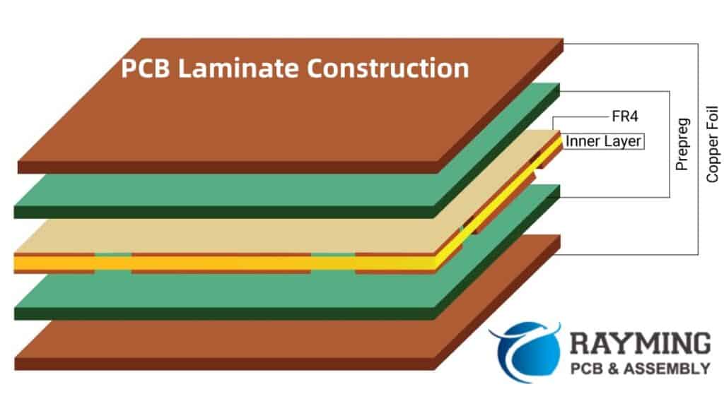
Substrate Core – The base structural layer granting mechanical support is a fiberglass reinforced laminate. Epoxy resin bonds stack layers. Popular base materials include FR-4 and CEM-3 which offer balance of performance and cost. More exotic substrates for high speed or RF use ceramic or polyimide films.
Conductive Copper Traces – Etched onto substrate core surfaces, these thin copper traces span between attached components to electrically link devices enabling transmission of power and signals between parts mounted on the PCB. Line widths vary based on current/density needs.
Pads & Vias – Contact pads provide component termination points. Holes called vias span layers making vertical connections through boards allowing traces on inner layers. These combine establishing electrical pathways across the PCB stackup.
Solder Mask – The solder mask is a polymer layer that coats copper traces providing insulation and preventing solder bridges. It features openings at pads to allow component terminals to solder to traces beneath while covering other conductor areas.
Silkscreen Legends – Often white print on PCB surfaces that indicate component placements, polarity markings, reference identifiers and other visual elements for assistance assembling boards.
Plating – At pads/holes, plating coats areas needing soldering or component connections. Common platings include HASL, ENIG or Immersion Silver over standard copper.
These materials fuse together forming multilayered PCBs housing electronics.
PCB Categorizations
Printed circuit boards breakdown into classifications based on attributes like number of conductive layers, substrate materials used, and fabrication process differences:
Single Sided – Budget boards with conductors only on one external side.
Double Sided – Copper traces on both external top and bottom sides. Vias span internally.
Multilayer – Constructed using multiple thin laminated substrate cores hosting trace layers externally and internally. Most complex designs.
Rigid PCB – Standard solid inflexible laminate substrates.
Flexible PCB – Using thin polymer bases allowing flexing and conforming PCBs.
HDI PCB – High density interconnect with tighter geometries allowing compact complex circuitry.
Aluminum or Metal Core – thermally conductive metal substrate base PCBs.
Hybrid PCBs – Combining different materials outlined above.
There exists many variations balancing performance, density, fabrication budget, and other priorities.
Core Functions
While serving as mechanical structure, the core functions provided by printed circuit boards span:
Physical Assembly & Alignment – The dimensional stability gives both through hole and surface mount components fixed anchoring placement to populate boards consistently.
Component Interconnections – Layers of etched traces directly link attached components routing flows of data, signals and power enabling all functionality.
Power Distribution – Certain layers often dedicate solely to distribute power rails evenly across large designs.
Shielding – Reference ground planes isolate signals across layers preventing coupling interference.
Heat Dissipation – Metal cores or thermal vias help conduct heat preventing detrimental elevated junction temps.
Environmental Protection – Conformal coatings applied to assembled PCBs shield against humidity, contaminants, vibration and other external threats.
The combinations of these abilities make PCBs centerpieces of electrical systems.
PCB Design and Layout

To produce a functional printed circuit board requires intentional planning and deliberate design practice:
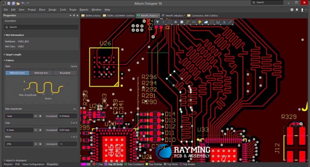
Schematics Design – Initially the schematic gets created showing logical component connectivity using electronic CAD software before PCB layout stages. This guides circuit needs.
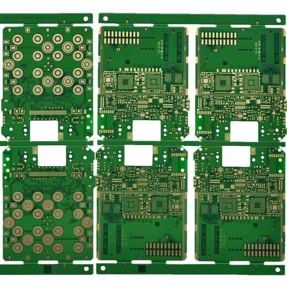
Board Shape – The mechanical dimensions meet physical size needs and panel utilization goals. Cutouts facilitate mounting.
Stackup Definition – Selecting core count along with layer thicknesses and materials targets functionality/cost balance. More layers enable complex routing.
Component Placement – Parts get positioned optimizing trace routing paths and design rules spacing considerations.
Routing Traces – Wires actually link parts placed on PCB layers like a roadmap establishing intended connectivity. May route manually or leverage autorouter assistance.
Validation Checks – Rigorous verification of clearances, EMC, signal integrity, manufacturability and assembly validates configuration meet all functional objectives.
Skills at each stage combine achieving an elegantly implemented PCB. Developers use electronic design automation software tools guiding the progression.
Fabrication and Assembly
Once PCB layout completes, design data outputs drive fabrication and assembly processes transforming boards into reality:
Fabrication – Complex chemical and mechanical processes start with bare laminate substrates then use photolithography masking and copper etching to selectively print conductive traces onto layers yielding finished boards. Additional drilling and plating steps produce mounting holes/vias. Meticulous precision ensures flawless electrical isolation between adjacent traces.
Assembly – Surface mount technology (SMT) and/or through hole assembly equipment populate printed boards positioning and soldering components onto pads accurately by running solder paste through reflow ovens melting solder or using wave soldering baths securing parts. Automated optical inspection checks for defects.
Testing and Validation – Fabricated assemblies undergo electrical testing probing nets, evaluating signal integrity metrics and ensuring quality standards match design intentions without faults before customer delivery.
Realizing functioning electronics requires integration of expertise spanning design conception through meticulous material sciences applied across realization procedures.
PCB Importance
Printed circuit boards continue growing in complexity and capabilities enabling breakthroughs powering innovations that transform products and entire industries:
- PCBs enabled miniaturized mobile consumer devices now ubiquitous worldwide
- Advanced HDI circuit boards accelerated computing leading the information revolution
- High frequency RF/microwave boards facilitated wireless everything connectivity
- Autonomous vehicle navigation relies on extremely high reliability vehicle boards
- Precision multilayer medical boards host life saving sensing functionality
Almost all modern electronics innovations connect back to printed circuit board technological capabilities evolving. The future remains bright as PCBs scale to integrate electronics deeper across more applications than ever.
Conclusion
A printed circuit board establishes the physical foundation on which almost any electronics subsystem gets constructed by providing firm mechanical structure and enabling layers of conductive traces printed on insulating substrates to route signals between attached components that collectively deliver system functionality. Understanding core elements constituting PCB compositions along with classifications, construction and assembly procedures provides broad awareness into this ubiquitous electronics necessity. Mastering foundational PCB literacy empowers grasping modern complex implementations that continue pushing technological possibilities improving life across industrial and consumer segments through relentlessly evolving electronic innovations.
Frequently Asked Questions
What are some key differences distinguishing rigid FR4 PCB substrates versus flexible PCB constructions?
Rigid FR4 PCBs use woven fiberglass reinforcement in the substrate laminate layers giving structural stability for standard through-hole and surface mount assembly. Flex PCBs instead utilize thin polymer films without reinforcement enabling bending and conforming abilities but limit components largely just to surface mounts.
Our mechanical engineers are asking if PCB substrate materials are compatible with high temperatures needed in our product enclosures?
There exists many substrate material formulations spanning FR-4, polyimides, ceramic, PTFE composites compatible with over 260°C lead-free soldering and high temperature enclosures above 150°C. The resin system glass transition temperature (Tg) determines max heat resistance. Select substrates appropriately.
We are researching options to enhance PCB reliability. What are pros and cons of ENIG versus Immersion Silver versus HASL surface finishes?
ENIG (electroless nickel immersion gold) offers excellent wear resistance sustaining reliable connectivity over cycles but higher initial cost. Immersion silver also boasts high durability and lower cost but some corrosion risks. HASL (hot air solder leveling) is budget friendly though less durable over long-term use scenarios.
What PCB characteristics are most important for RF microwave boards needed in our communications project?
Critical RF PCB properties look for tight dielectric constant tolerances and low Dk materials to ensure consistent electrical performance, precisely controlled trace impedances, ultra smooth copper and fine lines/spaces meeting wavelength needs, dense vias grids for shielding, and specialized connectors.
We want to embed electronics inside plastic enclosures. Are there PCB fabrication approaches enabling directly molding boards into plastics rather than needing fasteners?
Yes, injection molded PCBs allow molding thermoplastic materials directly around PCB substrate circuits utilizing specialized fabrication processes. This enables true 3D formed electronics rapid manufacturing.


Leave a Reply