Introduction to PCB Manufacturing
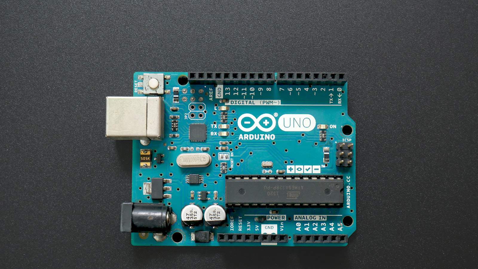
Printed Circuit Boards (PCBs) are the backbone of modern electronic devices. They are used in almost every electronic device, from smartphones and computers to medical equipment and automotive systems. PCBs provide a platform for electronic components to be connected and communicate with each other, enabling the device to function as intended. In this article, we will dive into the PCB manufacture process, exploring each step in detail.
The PCB Manufacture Process
The PCB manufacture process involves several steps, each of which is crucial to the final product’s quality and functionality. The process can be divided into the following stages:
- Design and Layout
- PCB Fabrication
- PCB Assembly
- Testing and Inspection
- Finishing and Packaging
Let’s explore each stage in more detail.
1. Design and Layout
The PCB manufacture process begins with the design and layout of the board. This stage involves creating a schematic diagram and a layout of the PCB using specialized software. The schematic diagram shows the electrical connections between the components, while the layout shows the physical placement of the components on the board.
The design and layout stage is critical because it determines the functionality and performance of the final product. The designer must consider factors such as signal integrity, power distribution, and thermal management when creating the layout.
2. PCB Fabrication
Once the design and layout are complete, the next stage is PCB fabrication. This stage involves several sub-processes, including:
2.1. Material Selection
The first step in PCB fabrication is selecting the appropriate material for the board. The most common material used for PCBs is FR-4, a glass-reinforced epoxy laminate. Other materials, such as polyimide or PTFE, may be used for high-frequency or high-temperature applications.
2.2. Copper Clad Laminate
The selected material is then coated with a thin layer of copper on one or both sides, depending on the design requirements. This copper layer will form the conductive paths on the PCB.
2.3. Drilling
After the copper clad laminate is prepared, holes are drilled through the board to allow for the insertion of components and vias. The drilling process is typically done using a computer-controlled drill machine.
2.4. Patterning
The next step is to create the conductive paths on the PCB by removing unwanted copper from the laminate. This is done using a process called etching. A photoresist layer is applied to the copper surface and exposed to light through a photomask, which contains the desired pattern. The exposed areas of the photoresist are then removed, leaving the copper exposed for etching.
2.5. Etching
The exposed copper is then removed using a chemical etching process, leaving only the desired conductive paths on the board.
2.6. Soldermask and Silkscreen
After etching, a soldermask layer is applied to the PCB to protect the copper traces from oxidation and prevent solder bridges during assembly. A silkscreen layer is then added to the board to provide labels and markings for the components.
3. PCB Assembly
With the fabrication process complete, the next stage is PCB assembly. This stage involves soldering the electronic components onto the board.
3.1. Solder Paste Application
The first step in PCB assembly is applying solder paste to the pads where the components will be placed. This is typically done using a stencil and a solder paste printer.
3.2. Component Placement
The components are then placed onto the board using a pick-and-place machine. This machine uses a vacuum nozzle to pick up the components and place them on the board with high precision.
3.3. Reflow Soldering
After the components are placed, the board goes through a reflow soldering process. The board is heated in an oven, causing the solder paste to melt and form a connection between the components and the pads.
4. Testing and Inspection
After assembly, the PCB undergoes thorough testing and inspection to ensure that it functions as intended and meets the required quality standards.
4.1. Automated Optical Inspection (AOI)
AOI is used to visually inspect the board for defects such as missing components, incorrect component placement, or solder bridges.
4.2. In-Circuit Testing (ICT)
ICT is used to test the functionality of the individual components on the board. This is done by applying electrical signals to the board and measuring the response.
4.3. Functional Testing
Functional testing is performed to ensure that the board performs as intended in its final application. This may involve testing the board in a simulated environment or integrating it into the final product for testing.
5. Finishing and Packaging
The final stage of the PCB manufacture process is finishing and packaging. This may involve applying additional coatings or treatments to the board for protection or aesthetic purposes. The board is then packaged and shipped to the customer.
Advantages of the PCB Manufacture Process
The PCB manufacture process offers several advantages, including:
- Consistency: The process is highly automated and standardized, ensuring consistent quality across multiple boards.
- Scalability: The process can be easily scaled up to produce large quantities of boards quickly and efficiently.
- Customization: The process allows for a high degree of customization, enabling designers to create boards tailored to specific applications.
- Reliability: The testing and inspection stages ensure that the final product is reliable and functions as intended.

Challenges in the PCB Manufacture Process
Despite its advantages, the PCB manufacture process also presents some challenges, such as:
- Complexity: As electronic devices become more complex, so do the PCBs that power them. This complexity can make the design and fabrication process more challenging.
- Miniaturization: The trend towards miniaturization in electronic devices requires PCBs to be smaller and more densely populated, which can be difficult to achieve.
- Material selection: Choosing the right material for a PCB can be challenging, as different materials have different properties and may not be suitable for all applications.
- Environmental concerns: The chemicals used in the PCB manufacture process can be harmful to the environment if not properly handled and disposed of.
Frequently Asked Questions (FAQ)
-
Q: How long does the PCB manufacture process typically take?
A: The lead time for PCB manufacturing can vary depending on the complexity of the board and the quantity being produced. Simple boards can be manufactured in a few days, while more complex boards may take several weeks. -
Q: What is the difference between single-sided and double-sided PCBs?
A: Single-sided PCBs have conductive paths on only one side of the board, while double-sided PCBs have conductive paths on both sides. Double-sided PCBs offer more space for components and can be more compact than single-sided boards. -
Q: What is the purpose of the soldermask layer on a PCB?
A: The soldermask layer serves two main purposes: it protects the copper traces from oxidation and prevents solder bridges from forming between adjacent pads during the assembly process. -
Q: Can PCBs be recycled?
A: Yes, PCBs can be recycled. The process involves separating the metal components from the board and recycling them separately. However, the recycling process can be complex and expensive, and not all recycling facilities have the capability to process PCBs. -
Q: What is the future of PCB manufacturing?
A: The future of PCB manufacturing is likely to involve continued miniaturization, increased use of advanced materials, and greater integration of embedded components. There is also a growing focus on sustainability and reducing the environmental impact of the manufacturing process.
Conclusion
The PCB manufacture process is a complex and multi-stage process that requires precision, skill, and attention to detail. From design and layout to fabrication, assembly, testing, and packaging, each stage plays a critical role in ensuring the final product meets the required quality and performance standards.
As electronic devices continue to evolve and become more complex, so too will the PCBs that power them. Manufacturers will need to stay up-to-date with the latest technologies and processes to meet the changing demands of the industry.
By understanding the PCB manufacture process and its advantages and challenges, designers and manufacturers can work together to create high-quality, reliable, and innovative electronic products that meet the needs of today’s consumers.
| Stage | Description |
|---|---|
| Design and Layout | Creating a schematic diagram and layout of the PCB using specialized software |
| PCB Fabrication | Producing the physical board, including material selection, copper clad laminate, drilling, patterning, etching, soldermask, and silkscreen |
| PCB Assembly | Soldering the electronic components onto the board, including solder paste application, component placement, and reflow soldering |
| Testing and Inspection | Ensuring the board functions as intended and meets quality standards, including automated optical inspection (AOI), in-circuit testing (ICT), and functional testing |
| Finishing and Packaging | Applying additional coatings or treatments to the board and packaging it for shipping to the customer |


Leave a Reply