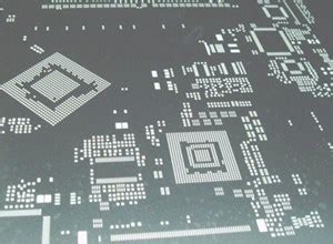
What are PCB Stencils?
PCB stencils, also known as solder paste stencils, are thin metal sheets with precisely cut openings that correspond to the pads on a PCB. These stencils are used to apply solder paste onto the PCB pads before the components are placed, ensuring a consistent and accurate application of solder paste.
Types of PCB Stencils
There are several types of PCB stencils available, each with its own advantages and disadvantages:
| Stencil Type | Description | Advantages | Disadvantages |
|---|---|---|---|
| Laser-cut | Cut using a high-precision laser | High accuracy, smooth edges | Higher cost, longer lead times |
| Electroformed | Created using a photographic process and electroplating | Excellent for fine-pitch applications | Fragile, higher cost |
| Chemically Etched | Etched using a chemical process | Lower cost, faster lead times | Lower accuracy, rough edges |
The Importance of PCB Stencils in Electronics Manufacturing
PCB stencils play a vital role in the surface mount technology (SMT) assembly process. They ensure the accurate and consistent application of solder paste onto the PCB pads, which is essential for achieving a reliable solder joint between the component and the PCB.
Benefits of Using PCB Stencils
-
Improved Solder Joint Quality: By applying a precise amount of solder paste, PCB stencils help create stronger and more reliable solder joints, reducing the risk of defects and failures.
-
Increased Production Efficiency: PCB stencils allow for the rapid application of solder paste, significantly reducing the time required for the assembly process.
-
Consistency and Repeatability: Stencils ensure that the same amount of solder paste is applied to each pad, resulting in a consistent and repeatable manufacturing process.

Factors to Consider When Choosing PCB Stencil Services
When selecting a PCB stencil service provider, several key factors should be considered to ensure the best results for your project:
1. Stencil Thickness
The thickness of the stencil is crucial for achieving the optimal amount of solder paste deposition. The ideal stencil thickness depends on various factors, such as the size of the components, the pitch of the pads, and the desired solder joint height.
| Component Size | Pitch | Recommended Stencil Thickness |
|---|---|---|
| 0402 and larger | ≥ 0.5mm | 0.125mm – 0.150mm |
| 0201 | 0.4mm – 0.5mm | 0.100mm – 0.125mm |
| 01005 | ≤ 0.4mm | 0.075mm – 0.100mm |
2. Stencil Material
The choice of stencil material depends on the specific requirements of your project. The most common materials used for PCB stencils are stainless steel and nickel. Stainless steel is the most widely used material due to its durability and cost-effectiveness, while nickel is preferred for fine-pitch applications due to its superior tensile strength and resistance to deformation.
3. Aperture Design
The aperture design of the stencil is critical for ensuring the correct amount of solder paste is deposited on each pad. Factors such as aperture size, shape, and wall angle should be carefully considered to achieve the desired solder paste volume and prevent issues such as bridging or insufficient solder paste deposition.
4. Stencil Coatings
Stencil coatings can be applied to improve the performance and durability of the stencil. Some common coatings include:
- Nano-coating: A hydrophobic coating that repels solder paste, preventing it from sticking to the stencil and improving transfer efficiency.
- Nickel plating: A protective coating that increases the wear resistance of the stencil and extends its lifespan.
5. Stencil Frame
The stencil frame provides support and stability to the stencil during the printing process. Factors to consider when choosing a stencil frame include:
- Frame size: The frame size should be compatible with your printing equipment and PCB dimensions.
- Frame material: Common frame materials include aluminum and stainless steel, each with its own advantages in terms of weight, durability, and cost.
- Mounting options: Stencil frames can be mounted using various methods, such as pneumatic clamping, magnetic clamping, or adhesive tape, depending on your printing equipment and preferences.

Advanced PCB Stencil Technologies
As the electronics industry continues to evolve, new technologies are emerging to meet the demands of increasingly complex PCB designs. Some of these advanced PCB stencil technologies include:
1. Step Stencils
Step stencils, also known as multi-level stencils, feature different thicknesses within a single stencil. This allows for the precise control of solder paste deposition on pads with varying sizes or heights, improving the overall quality of the solder joints.
2. 3D Printed Stencils
3D printing technology has recently been applied to the production of PCB stencils. This innovative approach enables the creation of complex stencil designs with intricate features, such as curved surfaces or variable aperture sizes, which are difficult or impossible to achieve with traditional stencil manufacturing methods.
3. Electroformed Nickel Stencils
Electroformed nickel stencils are created using a photographic process and electroplating, resulting in a high-precision stencil with excellent dimensional accuracy. These stencils are particularly well-suited for fine-pitch applications, where the smallest apertures and tightest tolerances are required.

Choosing the Right PCB Stencil Service Provider
With numerous PCB stencil service providers available, selecting the right one for your project can be a challenging task. Here are some key factors to consider when making your decision:
-
Experience and Expertise: Look for a service provider with a proven track record of delivering high-quality PCB stencils for a wide range of applications and industries.
-
Technology and Equipment: Ensure that the service provider invests in state-of-the-art technology and equipment to produce precise and reliable PCB stencils.
-
Quality Control: Choose a service provider that adheres to strict quality control standards and processes to ensure consistent and reliable results.
-
Customer Support: Select a service provider that offers excellent customer support, including responsive communication, technical assistance, and timely delivery.
-
Customization Options: Opt for a service provider that offers a wide range of customization options to meet the specific requirements of your project, such as different stencil materials, thicknesses, and coatings.
Frequently Asked Questions (FAQ)
-
What is the difference between a PCB stencil and a solder paste screen?
A PCB stencil and a solder paste screen are essentially the same thing. Both terms refer to a thin metal sheet with apertures that correspond to the pads on a PCB, used to apply solder paste during the SMT assembly process. -
How often should I replace my PCB stencil?
The lifespan of a PCB stencil depends on various factors, such as the stencil material, the type of solder paste used, and the frequency of use. As a general rule, stencils should be replaced when they show signs of wear, such as bent or damaged apertures, or when the print quality begins to deteriorate. -
Can I use the same PCB stencil for different solder paste types?
It is generally recommended to use a separate stencil for each type of solder paste to prevent cross-contamination and ensure optimal print quality. Different solder paste formulations may have different rheological properties, which can affect the transfer efficiency and print definition. -
How do I clean my PCB stencil?
PCB stencils should be cleaned regularly to remove excess solder paste and prevent the buildup of contaminants. The most common cleaning methods include manual cleaning with solvents and wiping materials, or automated cleaning using ultrasonic cleaners or stencil washing machines. -
What is the typical lead time for PCB stencil production?
The lead time for PCB stencil production varies depending on the complexity of the design, the chosen stencil material, and the workload of the service provider. Typical lead times range from 24 hours to several days, with expedited options available for urgent projects.
Conclusion
Advanced PCB and stencil services play a critical role in ensuring the quality, reliability, and efficiency of electronics manufacturing. By understanding the importance of PCB stencils, the factors to consider when choosing a stencil service provider, and the latest technologies available, you can make informed decisions that will help you achieve the best results for your project.
As the electronics industry continues to evolve, it is essential to stay up-to-date with the latest developments in PCB and stencil services. By partnering with a reputable and experienced service provider, you can leverage their expertise and technology to overcome the challenges of increasingly complex PCB designs and stay ahead of the competition.


Leave a Reply