Introduction to PCB Visualizer
In the world of electronics design, PCB (Printed Circuit Board) visualization plays a crucial role in ensuring the success of a project. A PCB Visualizer is a powerful tool that allows designers to create, modify, and analyze PCB layouts in a virtual environment before proceeding with the actual manufacturing process. This article will dive deep into the importance of PCB Visualizers, their features, and how they streamline the electronics design workflow.
What is a PCB Visualizer?
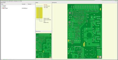
A PCB Visualizer is a software application that provides a graphical representation of a PCB layout. It allows designers to create, edit, and view PCB designs in a virtual environment, enabling them to identify and resolve issues before the board is manufactured. PCB Visualizers offer a range of features, including:
- Schematic capture: The ability to create and edit schematic diagrams of electronic circuits.
- PCB layout: Tools for placing and routing components on a virtual PCB.
- 3D visualization: Rendering of the PCB in a three-dimensional space for better visualization and analysis.
- Design rule checking (DRC): Automated checks to ensure that the PCB layout adheres to manufacturing constraints and design rules.
- Bill of Materials (BOM) generation: Automatic creation of a list of components used in the PCB design.
Benefits of Using a PCB Visualizer
Using a PCB Visualizer offers numerous benefits to electronics designers, including:
- Faster design process: PCB Visualizers allow designers to create and modify layouts quickly, reducing the overall design time.
- Improved accuracy: Automated design rule checks help identify and resolve issues before manufacturing, minimizing the risk of errors and reducing the need for costly revisions.
- Enhanced collaboration: PCB Visualizers enable easy sharing and collaboration among team members, facilitating efficient communication and faster decision-making.
- Cost savings: By identifying and resolving issues early in the design process, PCB Visualizers help reduce manufacturing costs and minimize the need for physical prototypes.
Key Features of PCB Visualizers
Schematic Capture
Schematic capture is the process of creating a graphical representation of an electronic circuit. PCB Visualizers provide tools for creating and editing schematic diagrams, allowing designers to define the connections between components and specify their properties. Schematic capture is an essential step in the PCB design process, as it serves as the foundation for the PCB layout.
PCB Layout
Once the schematic is created, designers can proceed with the PCB layout. PCB Visualizers offer a range of tools for placing and routing components on a virtual PCB. These tools include:
- Component placement: Placing components on the PCB based on their physical dimensions and electrical requirements.
- Trace routing: Creating electrical connections between components using copper traces.
- Via placement: Adding vias (vertical interconnect access) to connect traces on different layers of the PCB.
- Pad and footprint creation: Defining the size and shape of component pads and footprints.
PCB Visualizers also provide various display options, such as layer visibility control and color-coding, to enhance the visual representation of the layout.
3D Visualization
Many PCB Visualizers offer 3D visualization capabilities, allowing designers to view the PCB in a three-dimensional space. This feature provides a more realistic representation of the board, enabling designers to identify potential issues related to component placement, clearance, and mechanical interference. 3D visualization also facilitates communication with non-technical stakeholders, as it provides a more intuitive understanding of the PCB design.
Design Rule Checking (DRC)
Design Rule Checking (DRC) is an automated process that verifies the PCB layout against a set of predefined design rules. These rules ensure that the layout adheres to manufacturing constraints and industry standards, such as minimum trace width, spacing between components, and hole sizes. PCB Visualizers integrate DRC tools to identify and highlight any violations, allowing designers to make necessary adjustments before proceeding with manufacturing.
Bill of Materials (BOM) Generation
A Bill of Materials (BOM) is a comprehensive list of all the components used in a PCB design. PCB Visualizers can automatically generate a BOM based on the components placed in the layout. The BOM typically includes information such as component reference designators, manufacturer part numbers, quantities, and descriptions. Having an accurate BOM is crucial for procurement, assembly, and cost estimation purposes.

PCB Visualizer Workflow
The typical workflow when using a PCB Visualizer involves the following steps:
- Schematic capture: Create a schematic diagram of the electronic circuit, defining the components and their connections.
- Component placement: Place the components on the virtual PCB based on their physical dimensions and electrical requirements.
- Trace routing: Create electrical connections between components using copper traces, considering factors such as signal integrity and electromagnetic compatibility.
- Design rule checking: Run automated checks to ensure that the PCB layout adheres to manufacturing constraints and design rules.
- 3D visualization: View the PCB in a three-dimensional space to identify any mechanical or clearance issues.
- BOM generation: Generate a Bill of Materials based on the components used in the PCB design.
- Documentation: Create necessary documentation, such as assembly drawings and fabrication files, for manufacturing and assembly purposes.
By following this workflow, designers can efficiently create and refine PCB layouts, reducing the risk of errors and ensuring a smooth transition to the manufacturing phase.

Choosing the Right PCB Visualizer
When selecting a PCB Visualizer, designers should consider the following factors:
- Ease of use: The software should have a user-friendly interface and intuitive navigation to facilitate efficient design work.
- Feature set: Ensure that the PCB Visualizer offers the necessary features for your specific design requirements, such as schematic capture, 3D visualization, and DRC.
- Integration: Consider how well the PCB Visualizer integrates with other tools in your design workflow, such as CAD software and simulation tools.
- Compatibility: Verify that the PCB Visualizer supports the file formats and standards used in your industry or organization.
- Performance: Evaluate the software’s performance in terms of speed, stability, and ability to handle complex designs.
- Customer support: Look for a vendor that offers reliable customer support, documentation, and regular software updates.
By considering these factors, designers can choose a PCB Visualizer that best suits their needs and enables them to create high-quality PCB designs efficiently.

Best Practices for Using PCB Visualizers
To maximize the benefits of using a PCB Visualizer, designers should follow these best practices:
- Start with a clear schematic: Ensure that the schematic diagram accurately represents the intended circuit before proceeding with the PCB layout.
- Use a consistent naming convention: Adopt a consistent naming convention for components, nets, and layers to maintain clarity and organization throughout the design process.
- Follow design rules: Adhere to the manufacturing constraints and design rules specific to your industry or PCB fabrication provider to minimize the risk of manufacturing issues.
- Regularly run DRC: Perform design rule checks frequently throughout the design process to identify and resolve issues early on.
- Collaborate with team members: Leverage the collaboration features of PCB Visualizers to share designs, gather feedback, and ensure that all team members are working towards the same goal.
- Keep the layout organized: Use appropriate spacing, grouping, and labeling techniques to keep the PCB layout organized and readable.
- Verify the design in 3D: Utilize the 3D visualization capabilities to identify any mechanical or clearance issues that may not be apparent in a 2D view.
- Document the design: Create comprehensive documentation, including assembly drawings, fabrication files, and BOMs, to facilitate smooth communication with manufacturing and assembly teams.
By following these best practices, designers can ensure that their PCB designs are accurate, reliable, and ready for manufacturing.
Future Trends in PCB Visualization
As technology advances, PCB Visualizers are expected to evolve and offer even more sophisticated features to streamline the electronics design process. Some of the future trends in PCB visualization include:
- Artificial Intelligence (AI) integration: AI-powered tools can assist designers by suggesting optimal component placement, routing, and design rule adherence based on historical data and machine learning algorithms.
- Cloud-based collaboration: Cloud-based PCB Visualizers will enable seamless collaboration among geographically dispersed teams, allowing designers to access and modify designs from anywhere in the world.
- Virtual and Augmented Reality (VR/AR): VR and AR technologies can provide immersive experiences for visualizing and interacting with PCB designs, enhancing the design process and facilitating better communication with stakeholders.
- Integration with simulation tools: Tighter integration between PCB Visualizers and simulation tools will allow designers to perform real-time simulations and analyses directly within the visualization environment, enabling faster iterative design and optimization.
- Automated documentation: Advanced PCB Visualizers will offer automated documentation features, generating comprehensive reports, assembly instructions, and manufacturing files based on the PCB design.
By embracing these future trends, PCB Visualizers will continue to evolve and provide designers with powerful tools to create innovative and reliable electronic products.
Conclusion
PCB Visualizers have become an indispensable tool in the electronics design workflow, offering a range of features that streamline the creation, modification, and analysis of PCB layouts. By utilizing PCB Visualizers, designers can reduce design time, improve accuracy, enhance collaboration, and minimize the risk of manufacturing issues. As technology advances, PCB Visualizers are expected to incorporate even more sophisticated features, such as AI integration, cloud-based collaboration, and VR/AR capabilities, further empowering designers to create cutting-edge electronic products.
Frequently Asked Questions (FAQ)
-
What is the difference between a PCB Visualizer and a PCB design software?
A PCB Visualizer is a specific type of PCB design software that focuses on providing a graphical representation of the PCB layout. It offers features such as schematic capture, component placement, trace routing, and 3D visualization. PCB design software, on the other hand, is a broader term that encompasses various tools and functionalities used in the PCB design process, including PCB Visualizers. -
Can PCB Visualizers be used for complex, high-density PCB designs?
Yes, modern PCB Visualizers are capable of handling complex and high-density PCB designs. They offer advanced features such as multi-layer support, high-speed design tools, and automated routing algorithms to accommodate the requirements of complex designs. However, it is essential to choose a PCB Visualizer that is well-suited for your specific design complexity and industry standards. -
Are PCB Visualizers suitable for beginners in electronics design?
Many PCB Visualizers offer user-friendly interfaces and intuitive workflows, making them accessible to beginners in electronics design. Some PCB Visualizers also provide built-in libraries, design templates, and tutorials to help beginners get started. However, it is recommended that beginners familiarize themselves with the fundamentals of electronics design and PCB layout principles before diving into using a PCB Visualizer. -
How do PCB Visualizers handle design rule checking (DRC)?
PCB Visualizers integrate design rule checking (DRC) tools that automatically verify the PCB layout against a set of predefined design rules. These rules ensure that the layout adheres to manufacturing constraints and industry standards. The DRC tool highlights any violations and provides feedback to the designer, allowing them to make necessary adjustments. DRC is typically performed at various stages of the design process to catch and resolve issues early on. -
Can PCB Visualizers generate manufacturing files for PCB fabrication?
Yes, most PCB Visualizers can generate the necessary manufacturing files required for PCB fabrication. These files include Gerber files (for PCB layers), drill files (for hole locations), and pick-and-place files (for component placement). The PCB Visualizer generates these files based on the final PCB layout, ensuring that the design is accurately translated for manufacturing. It is crucial to verify the compatibility of the generated files with your chosen PCB fabrication provider.
| Feature | Description |
|---|---|
| Schematic Capture | Create and edit schematic diagrams of electronic circuits |
| PCB Layout | Place and route components on a virtual PCB |
| 3D Visualization | Render the PCB in a three-dimensional space for better visualization |
| Design Rule Checking | Automated checks to ensure the PCB layout adheres to manufacturing constraints |
| Bill of Materials (BOM) | Automatic generation of a list of components used in the PCB design |
By leveraging these features, designers can create accurate and efficient PCB layouts, reducing the risk of errors and streamlining the electronics design process.


Leave a Reply