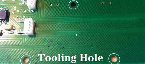
Introduction to PCB Drilled Holes
Printed Circuit Boards (PCBs) are essential components in modern electronics. They provide a platform for mounting and connecting electronic components, allowing for complex circuits to be designed and manufactured efficiently. One crucial aspect of PCB design and manufacturing is the creation of drilled holes, which serve various purposes such as component mounting, electrical connectivity, and mechanical support.
In this comprehensive article, we will dive deep into the world of PCB drilled holes, exploring their types, specifications, design considerations, and best practices. By understanding the intricacies of PCB drilled holes, you can ensure that your PCB designs are optimized for manufacturability, reliability, and functionality, avoiding costly surprises along the way.
Types of PCB Drilled Holes
There are several types of drilled holes commonly used in PCB design and manufacturing. Each type serves a specific purpose and has its own set of characteristics and requirements.
Through Holes
Through holes are the most common type of drilled holes in PCBs. They extend completely through the board, from one side to the other. Through holes are primarily used for mounting and soldering through-hole components, such as resistors, capacitors, and connectors. They also enable electrical connectivity between layers of the PCB.
Blind Vias
Blind vias are drilled holes that start from one surface of the PCB and terminate at a specific inner layer, without going through the entire board. They are used to connect an outer layer to one or more inner layers, providing electrical connectivity while saving space on the PCB surface.
Buried Vias
Buried vias are drilled holes that connect two or more inner layers of the PCB, without extending to either surface of the board. They are used to create connections between inner layers, allowing for more complex routing and higher component density.
Micro Vias
Micro vias are small, laser-drilled holes that are typically less than 0.15mm in diameter. They are used for high-density interconnects (HDI) and are commonly found in advanced packaging technologies such as chip-scale packages (CSPs) and ball grid arrays (BGAs).

PCB Drilled Hole Specifications
When designing and manufacturing PCBs, it is essential to understand and adhere to the specifications for drilled holes. These specifications ensure that the holes are properly sized, spaced, and positioned for optimal performance and manufacturability.
Hole Diameter
The diameter of a drilled hole is a critical specification that depends on the component lead size, the PCB thickness, and the manufacturing capabilities. Common hole diameters range from 0.2mm to 6.0mm, with smaller diameters used for high-density designs and larger diameters for power components or mechanical support.
| Component Type | Typical Hole Diameter Range |
|---|---|
| Resistors, Capacitors | 0.6mm – 1.0mm |
| Integrated Circuits (ICs) | 0.8mm – 1.2mm |
| Connectors | 1.0mm – 3.0mm |
| Power Components | 2.0mm – 6.0mm |
Hole Tolerance
Hole tolerance refers to the acceptable deviation from the specified hole diameter. It is essential to maintain tight tolerances to ensure proper component fit and solderability. The tolerance is typically expressed as a ± value, such as ±0.1mm.
Hole Placement Accuracy
Hole placement accuracy is the allowable deviation from the specified hole position on the PCB. This is critical for ensuring proper component alignment and preventing short circuits or open connections. The placement accuracy is usually specified in terms of a positional tolerance, such as ±0.05mm.
Aspect Ratio
The aspect ratio of a drilled hole is the ratio of the hole depth to its diameter. It is an important consideration for manufacturability, as high aspect ratios can be challenging to drill and plate properly. As a general rule, the aspect ratio should not exceed 10:1 for standard PCB manufacturing processes.

PCB Drilled Hole Design Considerations
When designing PCBs with drilled holes, there are several important considerations to keep in mind to ensure optimal performance, reliability, and manufacturability.
Pad Size and Annular Ring
The pad size and annular ring are crucial factors in ensuring proper solderability and mechanical strength of the drilled hole connection. The pad size should be large enough to accommodate the hole diameter and any positional tolerances. The annular ring, which is the copper area around the hole, should be wide enough to provide a strong mechanical connection and prevent pad lifting or delamination.
| Hole Diameter | Minimum Annular Ring |
|---|---|
| 0.2mm – 0.5mm | 0.125mm |
| 0.5mm – 1.0mm | 0.15mm |
| 1.0mm – 2.0mm | 0.2mm |
| 2.0mm – 6.0mm | 0.25mm |
Hole Spacing and Clearances
Proper hole spacing and clearances are essential for preventing short circuits, ensuring manufacturability, and maintaining signal integrity. The minimum spacing between holes depends on the PCB thickness, copper weight, and manufacturing capabilities. As a general guideline, the minimum hole-to-hole spacing should be at least 2 times the PCB thickness.
Drill Bit Selection and Maintenance
Selecting the appropriate drill bit size and material is crucial for achieving high-quality drilled holes. The drill bit should be slightly larger than the finished hole size to account for the plating thickness. Carbide drill bits are commonly used for their durability and ability to maintain precision over a large number of drilling cycles.
Regular maintenance and replacement of drill bits are essential for ensuring consistent hole quality and preventing drill breakage or damage to the PCB.
Plated vs. Non-Plated Holes
Plated holes are drilled holes that have a conductive copper layer deposited on the hole walls, providing electrical connectivity between layers. Non-plated holes, also known as mechanical holes, do not have a conductive layer and are used for component mounting or mechanical support.
When designing PCBs, it is essential to specify which holes should be plated and which should be non-plated, as this affects the manufacturing process and the final functionality of the board.

Best Practices for PCB Drilled Holes
To ensure optimal performance, reliability, and manufacturability of your PCB designs, consider the following best practices for drilled holes:
- Adhere to the minimum hole size and spacing guidelines provided by your PCB manufacturer.
- Use standard drill sizes whenever possible to reduce tooling costs and lead times.
- Avoid placing holes too close to the edge of the board or other components to prevent mechanical stress and damage.
- Specify the correct hole tolerance and placement accuracy for your application.
- Use plated holes for electrical connectivity and non-plated holes for mechanical support.
- Consider the aspect ratio of your drilled holes and design within the manufacturability limits.
- Communicate your drilled hole requirements clearly with your PCB manufacturer to avoid misunderstandings and delays.
Frequently Asked Questions (FAQ)
1. What is the difference between a through hole and a via?
A through hole extends completely through the PCB, from one side to the other, and is primarily used for mounting and soldering through-hole components. A via is a type of drilled hole that is used to connect different layers of the PCB, and it can be blind (starting from one surface and terminating at an inner layer) or buried (connecting inner layers without extending to either surface).
2. Can I use any drill size for my PCB holes?
While there is some flexibility in drill sizes, it is best to adhere to the standard drill sizes provided by your PCB manufacturer. Using standard sizes helps reduce tooling costs, improves manufacturability, and ensures the availability of the appropriate drill bits.
3. What is the minimum annular ring width for a drilled hole?
The minimum annular ring width depends on the hole diameter. As a general guideline, for hole diameters between 0.2mm and 0.5mm, the minimum annular ring should be 0.125mm. For larger hole diameters, the minimum annular ring width increases accordingly. However, it is essential to consult with your PCB manufacturer for their specific guidelines.
4. How do I ensure the proper alignment of drilled holes on my PCB?
To ensure proper alignment of drilled holes, it is essential to specify the correct hole placement accuracy in your design files. This is typically expressed as a positional tolerance, such as ±0.05mm. Additionally, using fiducial marks on your PCB design can help the manufacturer align the drill bits precisely.
5. Can I mix plated and non-plated holes on the same PCB?
Yes, you can have both plated and non-plated holes on the same PCB. Plated holes are used for electrical connectivity, while non-plated holes are used for mechanical support or component mounting. It is essential to clearly specify which holes should be plated and which should be non-plated in your design files to avoid confusion during manufacturing.
Conclusion
Drilled holes are a critical aspect of PCB design and manufacturing, serving various purposes such as component mounting, electrical connectivity, and mechanical support. Understanding the types of drilled holes, their specifications, design considerations, and best practices is essential for creating reliable, high-quality PCBs that meet your application’s requirements.
By adhering to the guidelines and best practices outlined in this comprehensive guide, you can avoid costly surprises and ensure that your PCB designs are optimized for manufacturability, reliability, and functionality. Remember to communicate your drilled hole requirements clearly with your PCB manufacturer, and don’t hesitate to seek their expertise and guidance when needed.
With this knowledge in hand, you are well-equipped to navigate the world of PCB drilled holes and create successful, high-performance electronic products.


Leave a Reply